| Introduction This document is not an in-depth presentation of the subject of electronics. Instead, it is intended to give you sufficient (empirical) knowledge of the subject to be able to understand, design and build simple circuits such as the control circuits used with the ‘Free Energy’ devices described in the later parts of this document. Disclaimer This material is provided for information purposes only. Should you decide to attempt construction of some device based on information presented here and injure yourself or any other person, I am not liable in any way. To clarify this; should you construct something in a heavy box and drop it on your toe, I am not liable for any injury you may sustain (you should learn to be more careful). If you attempt to construct some electronic circuit and burn yourself with the soldering iron, I am not liable. Also, I strongly recommend that unless you are expert in electronics, you do not construct any device using, or producing more than 12 Volts - high voltage circuits are extremely dangerous and should be avoided until you gain experience or can obtain the help and supervision of a person experienced in constructing high voltage circuits. Voltage Voltage is the key to understanding electronics. Without voltage, nothing happens in electronics. What is it? Nobody knows. We know how to generate it. We know what it does. We know how to measure it, but nobody knows what it actually is. It is also called “Electro Motive Force” or “EMF” which is no help whatsoever in knowing what it is. That, is roughly equivalent to saying “the thing that pushes is the thing that pushes” - very true but absolutely no help whatsoever. OK, having admitted that we really don't know what it is, we can start to say the things we do know about it: A new battery has a voltage between its terminals. This voltage is said to cause a current to flow through any complete electrical circuit placed across it. The current flowing through the circuit can cause various things to happen such as creating light, creating sound, creating heat, creating magnetism, creating movement, creating sparks, etc., etc. By using the current caused by a voltage, a device called a ‘Voltmeter’ can indicate how big the voltage is. The bigger the voltage, the bigger the current and the bigger the display on the voltmeter. The voltmeter can have a numerical display where you read the voltage directly from the display, or it can be an ‘analogue’ voltmeter where the voltage is shown by the position of a needle on a scale. The size of the voltage is stated in ‘Volts’ which is a unit of measurement named after the man Volta who introduced voltage to the world (it was always there, we just did not know about it). Voltages add up if they are connected the same way round, i.e. with the + terminals all facing the same way: 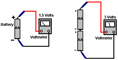 The physical size of the battery usually determines the length of time it can supply any given current - the bigger the battery, the longer it can provide any given current. A battery is constructed from a number of ‘cells’. The number of cells in the battery controls the voltage of the battery. For example, an ‘AA’ size battery (what used to be called a ‘penlight’ battery) has a single ‘cell’ and so produces 1.5 Volts when new. The very much larger and heavier ‘D’ battery also has just one cell and so it also produces 1.5 Volts when new. The difference (apart from the higher cost of the ‘D’ cell) is that the larger cell can provide a much higher current if both batteries are discharged over the same period of time. There are several different types of battery construction. A rechargeable NiCad battery has a single cell but its construction method means that it produces about 1.35 Volts when fully charged. In passing, NiCad batteries have a ‘memory’ characteristic which means that if they are recharged before they are fully discharged, then the next time they are discharged they run out of power at the voltage level it had when the last charging was started. Consequently, it is a good idea to fully discharge a NiCad battery before charging it again. Car and motorcycle batteries are described as Lead/Acid batteries. This type of construction is not very convenient being large, heavy and potentially corrosive. The big advantages are the ability to provide very high currents and giving 2.0 Volts per cell. These batteries are normally produced as 6 Volt or 12 Volt units. The Amp-Hours for lead/acid car batteries is usually quoted for a 20 hour discharge period, so a fully charged, new, 20 AHr battery can provide 1 Amp for 20 hours of continuous use. That battery loaded to give 5 Amps, will not provide that current for 4 hours but might only last 2 hours, or perhaps a little better. The manufacturers literature should give an indication of the performance, but if it is important, run your own test to see how the battery actually works in practice. “Mains units” are known in the electronics world as “Power Supply Units” or “PSUs” for short. These convert the mains voltage (220 Volts in UK, 110 Volts in USA) to some convenient low voltage; 12 Volts, 9 Volts, 6 Volts, or whatever is needed. A mains unit can provide several different voltages simultaneously. Resistance Being familiar with Voltage and Resistance is the key to understanding electronic circuitry. Resistance is a measure of how difficult it is for current to flow through something. Some materials such as glass, ceramics, wood and most plastics do not easily carry a current and so are considered to be ‘insulators’. That is why you will see power lines hung from their pylons by a series of ceramic discs. Current flows easily through metals, especially along the surface of the metal, so cables are made from metal wires surrounded by a layer of plastic insulation. The higher grade cables have wire cores made up of many small-diameter strands as this increases the surface area of the metal for any given cross-sectional area of the metal core (it also makes the cable more flexible, and generally, more expensive). There is a very important, third group of materials, silicon and germanium in particular, which fall between conductors and insulators. Not surprisingly, these are called ‘semi-conductors’ and the amount of current they can carry depends on the electrical conditions in which they are placed. Much, much more about this later on. While a metal wire carries current very well, it is not perfect at the job and so has some ‘resistance’ to current flowing through it. The thicker the wire, the lower the resistance. The shorter the wire, the lower the resistance. The first researchers used this characteristic to control the way circuits operated. Sometimes, as higher resistances were needed, the researcher used to need long lengths of wire which would get tangled up. To control the wire, a board with nails along each side was used and the wire wound backwards and forwards across the board like this: 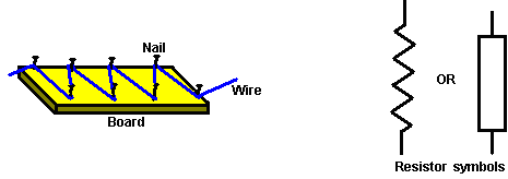 When drawing a circuit diagram, the researcher would sketch the wire on the board giving a zig-zag line which is still used today to represent a ‘resistor’ although different methods of construction are now used. An alternative symbol for a resistor is a plain rectangle as shown above. If a resistor is connected across a battery, a circuit is formed and a current flows around the circuit. The current cannot be seen but that does not mean that it is not there. Current is measured in ‘Amps’ and the instrument used to display it is an ‘ammeter’. If we place an ammeter in the circuit, it will show the current flowing around the circuit. In passing, the ammeter itself, has a small resistance and so putting it in the circuit does reduce the current flow around the circuit very slightly. Also shown is a bulb. If the current flowing around the circuit is sufficiently high and the bulb chosen correctly, then the bulb will light up, showing that current is flowing, while the ammeter will indicate exactly how much current is flowing: 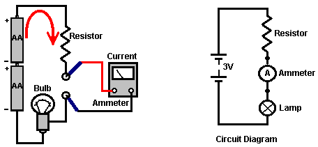 Shown on the right, is the way that this circuit would be shown by an electronics expert (the ‘Resistor’, ‘Ammeter’ and ‘Lamp’ labels would almost certainly not be shown). There are several different styles of drawing circuit diagrams, but they are the same in the basic essentials. One important common feature is that unless there is some very unusual and powerful reason not to do so, every standard style circuit diagram will have the positive voltage line horizontally at the top of the diagram and the negative as a horizontal line at the bottom. These are often referred to as the positive and negative ‘rails’. Where possible, the circuit is drawn so that its operation takes place from left to right, i.e. the first action taken by the circuit is on the left and the last action is placed on the right. Resistors are manufactured in several sizes and varieties. They come in ‘fixed’ and ‘variable’ versions. The most commonly used are the ‘fixed’ carbon ‘E12’ range. This is a range of values which has 12 resistor values which repeat: 10, 12, 15, 18, 22, 27, 33, 39, 47, 56, 68, 82 and then: 100, 120, 150, 180, 220, 270, 330, 390, 470, 560, 680, 820 and then: 1000, 1200, 1500, 1800, 2200, 2700, 3300, 3900, 4700, 5600, 6800, 8200, etc. etc. Nowadays, circuits often carry very little power and so the resistors can, and are, made in very small physical sizes. The higher the resistance value of a resistor, the less current will flow through it when a voltage is placed across it. As it can be difficult to see printing on small resistors clustered together on a circuit board and surrounded by other larger components, the resistor values are not written on the resistors, instead, the resistors are colour-coded. The unit of measurement for resistors is the ‘ohm’ which has a very small size. Most resistors which you encounter will be in the range 100 ohms to 1,000,000 ohms. The higher the resistance of any resistor, the smaller the current which will flow through it. The colour code used on resistors is: 0 Black 1 Brown 2 Red 3 Orange 4 Yellow 5 Green 6 Blue 7 Purple (Violet if your colour vision is very good) 8 Grey 9 White Each resistor has typically, three colour bands to indicate its value. The first two bands are the numbers and the third band is the number of noughts: 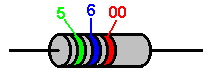 Green: 5 Blue: 6 Red: 2 noughts Value: 5,600 ohms or 5.6K 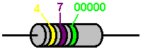 Yellow: 4 Purple: 7 Green: 5 noughts Value: 4,700,000 ohms or 4.7M or 4M7 The colour bands are read from left to right and the first band is close to one end of the body of the resistor. There is often a fourth band which indicates the manufacturing tolerance: you can ignore that band. Examples: Red, Red, Red: 2 2 00 ohms or 2K2 Yellow, Purple, Orange: 4 7 000 ohms or 47K Black, Brown, Brown: 1 0 0 ohms or 100R Orange, Orange, Orange: 3 3 000 ohms or 33K Brown, Green, Red: 1 5 00 ohms or 1K5 Brown, Green, Black: 1 5 no noughts, or 15 ohms Blue, Grey, Orange: 6 8 000 ohms or 68K Brown, Green, Green: 1 5 00000 ohms or 1,500,000 ohms or 1M5 Yellow, Purple, Brown: 4 7 0 ohms As there are only 12 standard resistor values per decade, there are only 12 sets of the first two colour bands: 10: Brown/Black 12: Brown/Red 15: Brown/Green 18: Brown/Grey 22: Red/Red 27: Red/Purple 33: Orange/Orange 39: Orange/White 47: Yellow/Purple 56: Green/Blue 68: Blue/Grey 82: Grey/Red   The details above give you all the basic information on resistor colour codes but there are a few additional refinements. There is an extra colour band further down the body of the resistor as shown here: 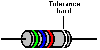 This extra band is used to indicate the manufacturing tolerance of the construction of the resistor. Resistor values are never exact and this rarely has any significant effect on their use in circuits. If some circuit needs very accurate resistor values in it, then buy several resistors of the same nominal value and use an ohm-meter to measure that actual value of each particular resistor and if none are perfect, then use two or more resistors to give the exact value wanted. The tolerance band has the following codes: Silver is ± 10% (i.e. a 10K resistor of this type should be between 9K and 11K) Gold ± 5% (i.e. a 10K resistor of this type should be between 9.5K and 10.5K) Red ± 2% (i.e. a 10K resistor of this type should be between 9.8K and 10.2K) Brown ± 1% (i.e. a 10K resistor of this type should be between 9.9K and 10.1K) Green ± 0.5% (i.e. a 10K resistor of this type should be between 9.95K and 10.05K) Blue ± 0.25% (i.e. a 10K resistor of this type should be between 9.975K and 10.025K) Purple ± 0.1% (i.e. a 10K resistor of this type should be between 9.99K and 10.01K) This type of resistor in the 10% and 5% ranges are the most common as they are the cheapest to buy and so tend to be the most popular. Recently, however, two additions to the coding have been introduced in order to allow for very high specification resistors which the average constructor may never come across. Each of these additions involves one additional colour band. The first additional colour band allows an extra digit in the resistor value, and looks like this: 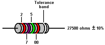 As before, the colour coding is exactly the same, with the fourth colour band specifying the number of zeros after the digits indicated by the colour bands in front of it. So, in the example shown above, the first band being Red indicates a "2". The second colour band being Purple indicates a "7". The third colour band being Green indicates a "5" and the fourth colour band being Red indicates "2 zeros", so putting those together it produces the value of 27,500 ohms, which can also be written as 27.5 K or more briefly as 27K5. Another example of this is: 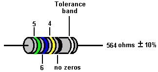 The fourth colour band coding has also been extended to include two other colours: Gold: meaning "no zeros and divided by 10" and Silver: meaning "no zeros and divided by 100". So, for example, if the resistor had a fourth colour band which was silver, then the value would be: 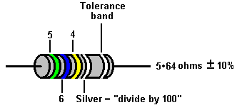 Finally, for very high-quality applications (typically military applications), there can be a sixth colour band positioned outside the tolerance band, and that final colour band states how much the resistance value can be expected to alter with changes in temperature. This is not something which is likely to be of any interest to you, but the codes for that final colour band are: Brown: 0.01% of the resistor value for each degree Centigrade change in temperature. Red: 0.005% of the resistor value for each degree Centigrade change in temperature. Yellow: 0.0025% of the resistor value for each degree Centigrade change in temperature. Orange: 0.0015% of the resistor value for each degree Centigrade change in temperature. To put this in context, the worst of these represents a change of 1% in the resistor value when moving from the temperature of ice to the temperature of boiling water. Is this something which you really care about? I don't. Leaving the details of identifying individual resistors, we now come to the interesting part: what happens when there are several resistors in a circuit. The important thing is to keep track of the voltages generated within the circuit. These define the currents flowing, the power used and the way in which the circuit will respond to external events. Take this circuit: 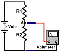 What is the voltage at point ‘A’? If you feel like saying “Who cares?” then the answer is “you” if you want to understand how circuits work, because the voltage at point ‘A’ is vital. For the moment, ignore the effect of the voltmeter used to measure the voltage. If R1 has the same resistance as R2, then the voltage at ‘A’ is half the battery voltage, i.e. 4.5 Volts. Half the battery voltage is dropped across R1 and half across R2. It does not matter what the actual resistance of R1 or R2 is, as long as they have exactly the same resistance. The higher the resistance, the less current flows, the longer the battery lasts and the more difficult it is to measure the voltage accurately. There is no need to do any calculations to determine the voltage at point “A” as it is the ratio of the resistor values which determines the voltage. If you really want to, you can calculate the voltage although it is not necessary. The method for doing this will be shown you shortly. For example, if R1 and R2 each have a value of 50 ohms, then the current flowing through them will be 9 volts / 100 ohms = 0.09 Amps (or 90 milliamps). The voltage drop across R1 will be 50 ohms = Volts / 0.09 amps or Volts = 4.5 volts. Exactly the same calculation shows that the voltage across R2 is exactly 4.5 volts as well. However, the point to be stressed here is that it is the ratio of R1 to R2 which controls the voltage at point “A”. If R1 has half as much resistance as R2, then half as much voltage is dropped across it as is dropped across R2, i.e. 3 Volts is dropped across R1, giving point ‘A’ a voltage of 6 Volts and that is what the voltmeter will show. Again, it does not matter what the actual value of R1 is in ohms, so long as R2 has exactly twice the resistance (shown by a higher number on the resistor). If R1 has twice as much resistance as R2, then twice as much voltage is dropped across it as is dropped across R2, i.e. 6 Volts is dropped across R1, giving point ‘A’ a voltage of 3 Volts. Here are some examples with different resistors: 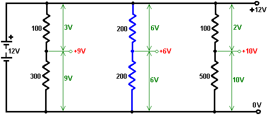 The same division of the supply voltage can be produced by positioning the slider of a variable resistor at different points by rotating the shaft of the device: 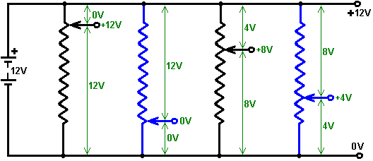 This principle applies immediately to the following circuit: 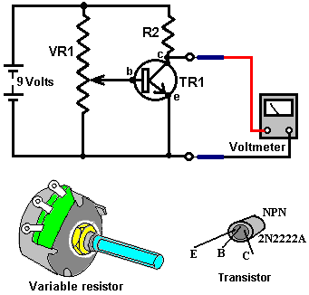 Here we encounter two new components. The first is ‘VR1’ which is a variable resistor. This device is a resistor which has a slider which can be moved from one end of the resistor to the other. In the circuit above, the variable resistor is connected across the 9 Volt battery so the top of the resistor is at 9 Volts and the bottom is at 0 Volts. The voltage on the slider can be adjusted from 0 Volts to 9 Volts by moving it along the resistor. The second new device is ‘TR1’ a transistor. This semiconductor has three connections: a Collector, a Base and an Emitter. If the base is disconnected, the transistor has a very high resistance between the collector and the emitter, much higher than the resistance of resistor ‘R1’. The voltage dividing mechanism just discussed means that the voltage at the collector will therefore, be very near to 9 Volts - caused by the ratio of the transistor’s Collector/Emitter resistance compared to the resistor “R2”. If a small current is fed from the base to the emitter, the resistance between the collector and the emitter drops almost instantly to a very low value, much, much lower than the resistance of resistor ‘R2’. This means that the voltage at the collector will be very close to 0 Volts. The transistor is described as having ‘switched on’. This state can be set by moving the slider of the variable resistor very slowly upwards to reach the switch-on point. This will be at a base/emitter voltage of 0.7 Volts, or so. The transistor can therefore be switched on and off just by rotating the shaft of the variable resistor. If a bulb is used instead of R2, then it will light when the transistor switches on. If a relay or opto-isolator is used, then a second circuit can be operated. If a buzzer is substituted for R2, then an audible warning will be sounded when the transistor switches on. If a opto-resistor is substituted for VR1, then the transistor will switch on when the light level increases or decreases, depending on how the sensor is connected. If a thermistor is used instead of VR1, then the transistor can be switched on by a rise or fall in temperature. Ditto, for sound, windspeed, water speed, vibration level, etc. etc. - more of this later. We need to examine the resistor circuit in more detail: 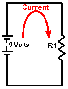 We need to be able to calculate what current is flowing around the circuit. This can be done using “Ohms Law” which states that “Resistance equals Voltage divided by Current” or, if you prefer: “Ohms = Volts / Amps” which indicates the units of measurement. In the circuit above, if the voltage is 9 Volts and the resistor is 100 ohms, then by using Ohm’s Law we can calculate the current flowing around the circuit as 100 Ohms = 9 Volts / Amps, or Amps = 9 / 100 which equals 0.09 Amps. To avoid decimal places, the unit of 1 milliamp is used. There are 1000 milliamps in 1 Amp. The current just calculated would commonly be expressed as 90 milliamps which is written as 90 mA. In the circuit above, if the voltage is 9 Volts and the resistor is 330 ohms, then by using Ohm’s Law we can calculate the current flowing around the circuit as 330 = 9 / Amps. Multiplying both sides of the equation by “Amps” gives: Amps x 330 ohms = 9 volts. Dividing both sides of the equation by 330 gives: Amps = 9 volts / 330 ohms which works out as 0.027 Amps, written as 27 mA. Using Ohm’s Law we can calculate what resistor to use to give any required current flow. If the voltage is 12 Volts and the required current is 250 mA then as Ohms = Volts / Amps, the resistor needed is given by: Ohms = 12 / 0.25 Amps which equals 48 ohms. The closest standard resistor is 47 ohms (Yellow / Purple / Black). The final thing to do is to check the wattage of the resistor to make sure that the resistor will not burn out when connected in the proposed circuit. The power calculation is given by: Watts = Volts x Amps. In the last example, this gives Watts = 12 x 0.25, which is 3 Watts. This is much larger than most resistors used in circuitry nowadays. Taking the earlier example, Watts = Volts x Amps, so Watts = 9 x 0.027 which gives 0.234 Watts. Again, to avoid decimals, a unit of 1 milliwatt is used, where 1000 milliwatts = 1 Watt. So instead of writing 0.234 Watts, it is common to write it as 234 mW. This method of working out voltages, resistances and wattages applies to any circuit, no matter how awkward they may appear. For example, take the following circuit containing five resistors: 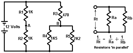 As the current flowing through resistor ‘R1’ has then to pass through resistor ‘R2’, they are said to be ‘in series’ and their resistances are added together when calculating current flows. In the example above, both R1 and R2 are 1K resistors, so together they have a resistance to current flow of 2K (that is, 2,000 ohms). If two, or more, resistors are connected across each other as shown on the right hand side of the diagram above, they are said to be ‘in parallel’ and their resistances combine differently. If you want to work out the equation above, for yourself, then choose a voltage across Rt, use Ohm’s Law to work out the current through Ra and the current through Rb. Add the currents together (as they are both being drawn from the voltage source) and use Ohm’s Law again to work out the value of Rt to confirm that the 1/Rt = 1/Ra + 1/Rb + .... equation is correct. A spreadsheet is included which can do this calculation for you. In the example above, R4 is 1K5 (1,500 ohms) and R5 is 2K2 (2,200 ohms) so their combined resistance is given by 1/Rt = 1/1500 + 1/2200 or Rt = 892 ohms (using a simple calculator). Apply a common-sense check to this result: If they had been two 1500 ohm resistors then the combined value would have been 750 ohms. If they had been two 2200 ohm resistors then the combined value would have been 1100 ohms. Our answer must therefore lie between 750 and 1100 ohms. If you came up with an answer of, say, 1620 ohms, then you know straight off that it is wrong and the arithmetic needs to be done again. So, how about the voltages at points ‘A’ and ‘B’ in the circuit? As R1 and R2 are equal in value, they will have equal voltage drops across them for any given current. So the voltage at point ‘A’ will be half the battery voltage, i.e. 6 Volts. Now, point ‘B’. Resistors R4 and R5 act the same as a single resistor of 892 ohms, so we can just imagine two resistors in series: R3 at 470 ohms and R4+R5 at 892 ohms. Common-sense rough check: as R3 is only about half the resistance of R4+R5, it will have about half as much voltage drop across it as the voltage drop across R4+R5, i.e. about 4 Volts across R3 and about 8 Volts across R4+R5, so the voltage at point ‘B’ should work out at about 8 Volts. We can use Ohm’s Law to calculate the current flowing through point ‘B’: Ohms = Volts / Amps, ( or Amps = Volts / Ohms or Volts = Ohms x Amps) (470 + 892) = 12 / Amps, so Amps = 12 / (470 + 892) Amps = 12 / 1362 or Amps = 0.00881 Amps (8.81 milliamps). Now that we know the current passing through (R4+R5) we can calculate the exact voltage across them: Resistance = Volts / Amps so 892 = Volts / 0.00881 or Volts = 892 x 0.00881 Volts = 7.859 Volts. As our common-sense estimate was 8 Volts, we can accept 7.86 Volts as being the accurate voltage at point ‘B’. The Potentiometer. Just before we leave the subject of resistors and move on to more interesting subjects, we come across the term ‘potentiometer’. This term is often shortened to ‘pot’ and many people use it to describe a variable resistor. I only mention this so that you can understand what they are talking about. A variable resistor is not a potentiometer and really should not be called one. You can skip the rest of this part as it is not at all important, but here is what a potentiometer is: A fancy name for voltage is ‘potential’, so a circuit powered by a 12 Volt battery can be described as having a ‘potential’ of zero volts at the negative side of the battery and a ‘potential’ of plus twelve volts at the positive side of the battery. Ordinary folks like me would just say ‘voltage’ instead of ‘potential’. When a voltmeter is used to measure the voltage at any point in a circuit, it alters the circuit by drawing a small amount of current from the circuit. The voltmeter usually has a high internal resistance and so the current is very small, but even though it is a small current, it does alter the circuit. Consequently, the measurement made is not quite correct. Scientists, in years gone by, overcame the problem with a very neat solution - they measured the voltage without taking any current from the circuit - neat huh? They also did it with a very simple arrangement:  They used a sensitive meter to measure the current. This meter is built so that the needle is in a central position if no current is flowing. With a positive current flowing, the needle deflects to the right. With a negative current flowing, the needle moves to the left. They then connected a variable resistor ‘VR1’ across the same battery which was powering the circuit. The top end of VR1 is at +12 Volts (they called that ‘a potential of +12 Volts’) and the bottom end of VR1 is at zero volts or ‘a potential of zero volts’. By moving the slider of VR1, any voltage or ‘potential’ from zero volts to +12 Volts could be selected. To measure the voltage at point ‘A’ without drawing any current from the circuit, they would connect the meter as shown and adjust the variable resistor until the meter reading was exactly zero. Since the meter reading is zero, the current flowing through it is also zero and the current taken from the circuit is zero. As no current is being taken from the circuit, the measurement is not affecting the circuit in any way - very clever. The voltage on the slider of VR1 exactly matches the voltage at point ‘A’, so with a calibrated scale on the variable resistor, the voltage can be read off. The slick piece of equipment made up from the battery, the variable resistor and the meter was used to measure the ‘potential’ (voltage) at any point and so was called a ‘potentiometer’. So, please humour me by calling a variable resistor a ‘variable resistor’ and not a ‘potentiometer’. As I said before, this is not at all important, and if you want to, you can call a variable resistor a ‘heffalump’ so long as you know how it works. Semiconductors This section deals with discrete semiconductors. A later section deals with ‘Integrated Circuits’ which are large-scale semiconductor devices. The ORP12 Light-dependent resistor. This device has a high resistance in the dark and a low resistance in bright light. It can be placed in a circuit to create a switch which operates with an increase in light level or a decrease in light level:  In this version, the voltage at point ‘A’ controls the circuit. In darkness, the ORP12 has a resistance ten times greater than that of R1 which is 12,000 ohms. Consequently, the voltage at point ‘A’ will be high. As the light level increases, the resistance of the ORP12 falls, dragging the voltage at point ‘A’ downwards. As the variable resistor ‘VR1’ is connected from point ‘A’ to the ground rail (the -ve of the battery), its slider can be moved to select any voltage between 0 Volts and the voltage of ‘A’. A slider point can be chosen to make the transistor switch off in daylight and on at night. To make the circuit trigger when the light level increases, just swap the positions of R1 and the ORP12. The transistor shown is a BC109 although most transistors will work in this circuit. The BC109 is a cheap, silicon, NPN transistor. It can handle 100mA and 30V and can switch on and off more than a million times per second. It has three connections: the Collector, marked ‘c’ in the diagram, the Base, marked ‘b’ in the diagram and the Emitter, marked ‘e’ in the diagram. As mentioned before, it has a very high resistance between the collector and the emitter when no current flows into the base. If a small current is fed into the base, the collector/emitter resistance drops to a very low value. The collector current divided by the base current is called the ‘gain’ of the transistor and is often called ‘hfe’. A transistor such as a BC109 or a BC108 has a gain of about 200, though this varies from actual transistor to actual transistor. A gain of 200 means that a current of 200mA passing through the collector requires a current of 1mA through the base to sustain it. Specific information on the characteristics and connections of semiconductors of all kinds can be obtained free from the excellent website which provides .pdf information files. The BC109 transistor shown above is an NPN type. This is indicated by the arrow of the symbol pointing outwards. You can also tell by the collector pointing to the positive rail. There are similar silicon transistors constructed as PNP devices. These have the arrow in the transistor symbol pointing inwards and their collectors get connected, directly or indirectly, to the negative rail. This family of transistors are the earliest transistor designs and are called ‘bi-polar’ transistors. These silicon transistors are so efficiently constructed that they can be connected directly together to give greatly increased gain. This arrangement is called a ‘Darlington pair’. If each transistor has a gain of 200, then the pair give a gain of 200 x 200 = 40,000. This has the effect that a very, very small current can be used to power a load. The following diagram shows a Darlington pair used in a water-level detector. This type of alarm could be very useful if you are asleep on a boat which starts taking on water.  Here, (when the circuit is switched on), transistor TR1 has so little leakage current that TR2 is starved of base current and is hard off, giving it a high resistance across its collector/emitter junction. This starves the buzzer of voltage and keeps it powered off. The sensor is just two probes fixed in place above the acceptable water level. If the water level rises, the probes get connected via the water. Pure water has a high electrical resistance but this circuit will still work with pure water. The odds are that in a practical situation, the water will not be particularly clean. The resistor R1 is included to limit the base current of TR1 should the sensor probes be short-circuited. Silicon bi-polar transistors have a base/emitter voltage of about 0.7V when fully switched on. The Darlington pair will have about 1.4V between the base of TR1 and the emitter of TR2, so if the sensor probes are short-circuited together, resistor R1 will have 6 - 1.4 = 4.6V across it. Ohms Law gives us the current through it as R = V / A or 47,000 = 4.6 / A or A = 4.6 / 47,000 amps. This works out at 0.098mA which with a transistor gain of 40,000 would allow up to 3.9A through the buzzer. As the buzzer takes only 30mA or so, it limits the current passing through it, and TR2 can be considered to be switched hard on with the whole battery voltage across it. NPN transistors are more common than PNP types but there is almost no practical difference between them. Here is the previous circuit using PNP transistors: 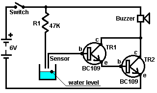 Not a lot of difference. Most of the circuit diagrams shown here use NPN types but not only are these not critical, but there are several ways to design any particular circuit. In general, the semiconductors shown in any circuit are seldom critical. If you can determine the characteristics of any semiconductor shown, any reasonably similar device can generally be substituted, especially if you have a general understanding of how the circuit works. Either of the two previous circuits can operate as a rain detector. A suitable sensor can easily be made from a piece of strip board with alternate strips connected together to form an interlacing grid: 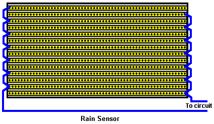 Here, if a raindrop bridges between any two adjacent strips, the circuit will trigger and sound a warning. The transistors in the circuit above are connected with their emitter(s) connected to the ground rail (the lower battery line shown in any circuit is considered to be “ground” unless it is specifically shown elsewhere). This connection method is called ‘common emitter’. The following circuit uses the transistor connected in ‘emitter follower’ mode. This is where the emitter is left to follow the base voltage - it is always 0.7V below it unless the base itself is driven below 0.7V: 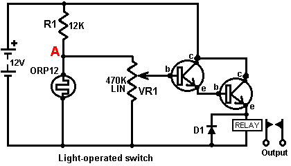 This is almost the same as the light-operated circuit shown earlier. In this variation, the transistors are wired so that they work as an ‘emitter-follower’ which follows the voltage at point ‘A’ which rises as the light level drops and the resistance of the ORP12 increases. This causes the voltage across the relay to increase until the relay operates and closes its contacts. A relay is a voltage-operated mechanical switch which will be described in more detail later on. The disadvantage of the above circuit is that as the light level decreases, the current through the relay increases and it may be a significant amount of current for some considerable time. If it was intended to power the unit with a battery then the battery life would be far shorter than it need be. What we would like, is a circuit which switched rapidly from the Off state to the On state even though the triggering input varied only slowly. There are several ways to achieve this, one of them being to modify the circuit to become a ‘Schmitt Trigger’: 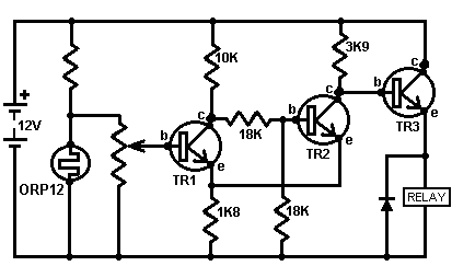 Here, an additional transistor (‘TR2’) has changed the circuit operation significantly, with transistor TR3 switching fully on and fully off, rapidly. This results in the current through the relay being very low until the circuit triggers. The circuit operates as follows. When the voltage at the base of TR1 is high enough, TR1 switches on, which causes the resistance between its collector and emitter to be so low that we can treat it as a short circuit (which is a nearly-zero resistance connection). This effectively connects the 10K and 1K8 resistors in series across the battery. The voltage at their connecting point (both the collector and emitter of TR1) will then be about 1.8 Volts. The two 18K resistors are in series across that voltage so the voltage at their junction will be half that; 0.9 Volts. This puts the Base of TR2 at about 0.9 Volts and its emitter at 1.8 Volts. The base of TR2 is therefore not 0.7 Volts above its emitter, so no base/emitter current will flow in TR2, which means that TR2 is switched hard off. This means that the TR2 collector/emitter resistance will be very high. The voltage at the base of TR3 is controlled by the 1K8 resistor, the TR2 collector/emitter resistance (very high) and the 3K9 resistor. This pushes the base voltage of TR3 up to near the full battery voltage and as it is wired as an emitter-follower, its emitter voltage will be about 0.7 Volts below that. This means that the relay will have most of the battery voltage across it and so will switch hard on. Some practical points: The current flowing into the base of TR3 comes via the 3K9 resistor. A 3K9 resistor needs 3.9 Volts across it for every 1 mA which flows through it. If the relay needs 150 mA to operate and TR3 has a gain of 300, then TR3 will need a base current of 0.5 mA to provide 150 mA of current through its collector/emitter junction. If 0.5 mA flows through the 3K9 resistor, there will be a voltage drop across it of some 2 Volts. The TR3 base/emitter voltage will be a further 0.7 Volts, so the voltage across the relay will be about 12.0 - 2.0 - 0.7 = 9.3 Volts, so you need to be sure that the relay will work reliably at 9 Volts. If you used a Darlington pair of transistors, each with a gain of 300, instead of TR3, then their combined base/emitter voltage drop would be 1.4 Volts, but they would only need a base current of 150 mA / (300 x 300) = 1/600 mA. That current would only drop 0.007 Volts across the 3K9 resistor, so the relay would receive 10.6 Volts. So, how do you work out the gain of any particular transistor? The main working tool for electronics is a multimeter. This is a digital or analogue meter which can measure a wide range of things: voltage, current, resistance, ... The more expensive the meter, generally, the greater the number of ranges provided. The more expensive meters offer transistor testing. Personally, I prefer the older, passive multimeters. These are looked down on because they draw current from the circuit to which they are attached, but, because they do, they give reliable readings all the time. The more modern battery-operated digital multimeters will happily give incorrect readings as their battery runs down. I wasted two whole days, testing rechargeable batteries which appeared to be giving impossible performances. Eventually, I discovered that it was a failing multimeter battery which was causing false multimeter readings. For the moment, let us assume that no commercial transistor tester is to hand and we will build our own (or at least, discover how to build our own). The gain of a transistor is defined as the collector/emitter current divided by the base/emitter current. For example, if 1mA is flowing through the collector and 0.01mA is flowing into the base to sustain that collector flow, then the transistor has a gain of 100 times at 1mA. The transistor gain may vary when it is carrying different current loads. For the circuits we have been looking at so far, 1mA is a reasonable current at which to measure the transistor gain. So let’s build a circuit to measure the gain: 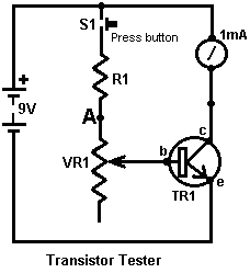 With the circuit shown here, the variable resistor is adjusted until a collector current of 1mA is shown on the milliammeter and the gain of the transistor is then read off the scale on the variable resistor knob. The circuit is built into a small box containing the battery and with a socket into which the transistor can be plugged. The question then is, what values should be chosen for the resistor R1 and the variable resistor VR1? Well, we might choose that the minimum gain to be displayed is 10. This would correspond to where the variable resistor slider is taken all the way up to point ‘A’ in the circuit diagram, effectively taking the variable resistor out of the circuit. If the transistor gain is 10 and the collector current is 1mA, then the base current will be 0.1mA. This current has to flow through the resistor R1 and it has a voltage of (9.0 - 0.7) Volts across it as the base/emitter voltage is 0.7 Volts when the transistor is on. Ohms Law gives us Ohms = Volts / Amps, which for the resistor R1 means Ohms = 8.3 / 0.0001 or 83,000 ohms, or 83K. Rule of thumb: 1K provides 1mA if it has 1V across it, so 10K will give 0.1mA if it has 1 Volt across it. With 8.3 Volts across it, it needs to be 8.3 times larger to hold the current down to the required 0.1mA so the resistor should be 83K in size. As 83K is not a standard size, we need to use two or more standard resistors to give that resistance. Nearest standard size below 83K is 82K, so we can used one 82K resistor and one 1K resistor in series to give the required 83K. Suppose that we say that we would like to have 500 as the highest gain shown on our tester, then when VR1 is at its maximum value, it and R1 should provide 1/500 of the collector current of 1mA, i.e. 0.002mA or 0.000002 Amps. From Ohms Law again we get VR1 + R1 = 4,150,000 ohms or 4M15. Unfortunately, the largest value variable resistor available is 2M2 so the circuit as it stands, will not be able to cope. Suppose we were to just use a 2M2 variable resistor for VR1, what transistor gain range could we display? Well Ohms Law ... lets us calculate the base current with 8.3 Volts across (83,000 + 2,200,000) ohms and from that the maximum transistor gain which would be 277.77 (at 1mA). You would buy a ‘linear’ standard carbon track variable resistor so that the change in resistance is steady as the shaft is rotated. The scale which you would make up would be in even steps and it would run from 10 at the minimum setting, to 278 at the highest setting. But that is not what we wanted. We wanted to measure up to 500. But they don’t make variable resistors big enough, so what can we do? Well, if we wanted, we could lower the battery voltage, which in turn would lower the resistor values. As a 9V battery is very convenient for this kind of circuit, lets not go down that route. We could add extra circuitry to drop the 9V battery voltage down to a lower value. The most simple solution is to add an extra resistor and switch to give two ranges. If we switched in an extra 2M2 resistor above VR1 then the circuit would measure transistor gains from 278 to just over 500 and all we would need to do would be to add a second scale for the VR1 pointer knob to move over. We could, provide extra ranges which overlap and which have more convenient scales to mark. The design is up to you. 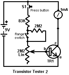 The design covered above is not the only way to measure the transistor gain. A second way, which accepts that it is not so accurate, picks a set base current and measures the collector current as a guide to the gain. In this simple method, one or more resistor values are chosen to give gain ranges, and the milliammeter used to read the corresponding gain: 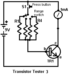 Here, resistor R1 might be chosen to give a collector current of 1mA (which is a full-scale deflection on the meter) when the transistor gain is 100. Resistor R2 might be picked to give a full-scale deflection for a gain of 200, R3 for a gain of 400, R4 for a gain of 600, and so on. Generally speaking, it is not essential to know the exact gain but any reasonable approximation to it is sufficient. You are normally selecting a transistor where you need a gain of 180, so it is not important if the transistor you pick has a gain of 210 or 215 - you are only avoiding transistors with gains below 180. How do you work out the values of the resistors R1 to R4? Well, you probably won’t expect this, but you use Ohms Law. Voltage drop is 8.3 Volts and the base current is given by the full-scale deflection’s 1mA divided by the transistor gain for each range, i.e. 1/100 mA for R1, 1/200 mA for R2,... 1/600 mA for R4,... The Diode One component which has been shown but not described is the diode or ‘rectifier’. This is a device which has a very high resistance to current flowing in one direction and a very low resistance to current flowing in the opposite direction. The base/emitter junction of a transistor is effectively a diode and, at a push, can be used as such. A proper diode is cheap to buy and has far greater voltage and current handling capacities than the base/emitter junction of a transistor. Diodes are mainly made from one of two materials: germanium and silicon. Germanium diodes are used with very small alternating currents such as radio signals coming from an aerial. This is because a germanium diode needs only 0.2 Volts or so to carry a current while silicon needs 0.6 to 0.7 Volts (same as a silicon transistor base/emitter junction). Germanium diodes (and transistors) are very sensitive to temperature change and so are normally restricted to low power circuits. One very neat application for a silicon diode is as an ‘un-interruptible power supply’ where mains failure is caught instantly: 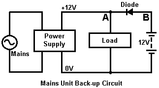 In this circuit, the mains voltage drives the Power Supply Unit which generates 12 Volts at point ‘A’. This provides current to the Load. The diode has +12 Volts at ‘A’ and +12 Volts at point ‘B’ so there is no voltage drop across it and it will not carry current in either direction. This means that the battery is effectively isolated when the mains is functioning. If the Power Supply Unit output were to rise above its design level of +12 Volts, then the diode would block it from feeding current into the battery. If the mains fails, the Power Supply Unit (‘PSU’) output will fall to zero. If the battery and diode were not there, the voltage at point ‘A’ would fall to zero, which would power-down the Load and possibly cause serious problems. For example, if the load were your computer, a mains failure could cause you to lose important data. With a battery back-up of this type, you would have time to save your data and shut your computer down before the battery ran out. The circuit operates in a very simple fashion. As soon as the voltage at point ‘A’ drops to 0.7 Volts below the +12 Volts at point ‘B”, the diode starts feeding current from the battery to the Load. This happens in less than a millionth of a second, so the Load does not lose current. It would be worth adding a warning light and/or a buzzer to show that the mains has failed. 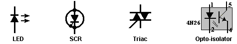 LEDs: There is a widely used variation of the diode which is extremely useful, and that is the Light Emitting Diode or ‘LED’. This is a diode which emits light when carrying current. They are available in red, green, blue, yellow or white light versions. Some versions can display more than one colour of light if current is fed through their different electrical connections. LEDs give a low light level at a current of about 8 or 10 mA and a bright light for currents of 20 to 30 mA. If they are being used with a 12 Volt system, then a series resistor of 1K to 330 ohms is necessary. LEDs are robust devices, immune to shock and vibration. They come in various diameters and the larger sizes are very much more visible than the tiny ones. SCRs and Triacs: Another version of the diode is the Silicon Controlled Rectifier or ‘Thyristor’. This device carries no current until its gate receives an input current. This is just like the operation of a transistor but the SCR once switched on, stays on even though the gate signal is removed. It stays on until the current through the SCR is forced to zero, usually by the voltage across it being removed. SCRs are often used with alternating voltages (described below) and this causes the SCR to switch off if the gate input is removed. SCRs only operate on positive voltages so they miss half of the power available from alternating power supplies. A more advanced version of the SCR is the ‘Triac’ which operates in the same way as an SCR but handles both positive and negative voltages. Opto-Isolators: Another very useful variation on the LED is the Opto-Isolator. This device is a fully enclosed LED and light-sensitive transistor. When the LED is powered up, it switches the transistor on. The big advantage of this device is that the LED can be in a low voltage, low power sensing circuit, while the transistor can be in a completely separate, high voltage, high power circuit. The opto-isolator isolates the two circuits completely from each other. It is a very useful, and very popular, low-cost device. Alternating Current: A battery provides a constant voltage. This is called a Direct Current or ‘DC’ source of power. When a circuit is connected to a battery, the positive rail is always positive and the negative rail is always negative. If you connect a battery to a circuit through a double-pole changeover switch as shown here: 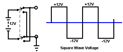 When the changeover switch is operated, the battery is effectively turned over or inverted. This circuit is called an ‘inverter’ because it repeatedly inverts the supply voltage. If the switch is operated on a regular, rapid basis, the graph of the output voltage is as shown on the right. This is a ‘square wave’ voltage and is used extensively in electronic equipment. It is called alternating current or ‘AC’ for short. SCRs and Triacs can be used conveniently with supply voltages of this type. Mains voltage is also AC but is rather different: 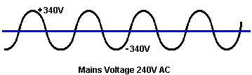 Mains voltage varies continuously in the form of a sine wave. In Britain, the mains voltage is described as ‘240 Volts AC’ and it cycles up and down 50 times per second, i.e. 50 positive peaks and 50 negative peaks in one second. It would be reasonable to assume that each voltage peak would be 240 Volts but this is not the case. Even though the supply is described as 240 Volts, it peaks at the square root of 2 times greater than that, i.e. 339.4 Volts. The actual supply voltage is not particularly accurate, so any device intended for mains use should be rated to 360 Volts. In America, the supply voltage is 110 Volts AC and it cycles 60 times per second, peaking at plus and minus 155 Volts. Later on, you will see how one or more diodes can be used to convert AC to DC in a unit which is sold as a ‘mains adapter’ intended to allow battery operated equipment be operated from the local mains supply. Coils: If you take a cardboard tube, any size, any length, and wind a length of wire around it, you create a very interesting device. It goes by the name of a ‘coil’ or an ‘inductor’ or a ‘solenoid’. 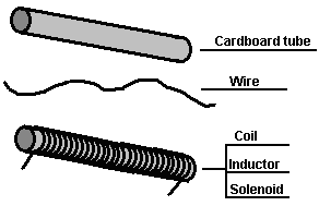 This is a very interesting device with many uses. It forms the heart of a radio receiver, it used to be the main component of telephone exchanges, and most electric motors use several of them. The reason for this is if a current is passed through the wire, the coil acts in exactly the same way as a bar magnet: 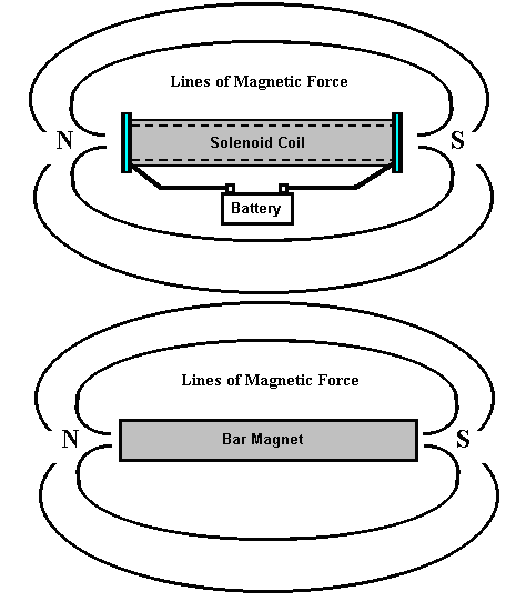 The main difference being that when the current is interrupted, the coil stops acting like a magnet, and that can be very useful indeed. If an iron rod is placed inside the coil and the current switched on, the rod gets pushed to one side. Many doorbells use this mechanism to produce a two-note chime. A ‘relay’ uses this method to close an electrical switch and many circuits use this to switch heavy loads (a thyristor can also be used for this and it has no moving parts). A coil of wire has one of the most peculiar features of almost any electronic component. When the current through it is altered in any way, the coil opposes the change. Remember the circuit for a light-operated switch using a relay?:  You will notice that the relay (which is mainly a coil of wire), has a diode across it. Neither the relay nor the diode were mentioned in any great detail at that time as they were not that relevant to the circuit being described. The diode is connected so that no current flows through it from the battery positive to the ‘ground’ line (the battery negative). On the surface, it looks as if it has no use in this circuit. In fact, it is a very important component which protects transistor TR3 from damage. The relay coil carries current when transistor TR3 is on. The emitter of transistor TR3 is up at about +10 Volts. When TR3 switches off, it does so rapidly, pushing the relay connection from +10 Volts to 0 Volts. The relay coil reacts in a most peculiar way when this happens, and instead of the current through the relay coil just stopping, the voltage on the end of the coil connected to the emitter of TR3 keeps moving downwards. If there is no diode across the relay, the emitter voltage is forced to briefly overshoot the negative line of the circuit and gets dragged down many volts below the battery negative line. The collector of TR3 is wired to +12 Volts, so if the emitter gets dragged down to, say, -30 Volts, TR3 gets 42 Volts placed across it. If the transistor can only handle, say, 30 Volts, then it will be damaged by the 42 Volt peak. The way in which coils operate seems weird. But, knowing what is going to happen at the moment of switch-off, we deal with it by putting a diode across the coil of the relay. At switch-on, and when the relay is powered, the diode has no effect, displaying a very high resistance to current flow. At switch-off, when the relay voltage starts to plummet below the battery line, the diode effectively gets turned over into its conducting mode. When the voltage reaches 0.7 Volts below the battery negative line, the diode starts conducting and pins the voltage to that level until the voltage spike generated by the relay coil has dissipated. The more the coil tries to drag the voltage down, the harder the diode conducts, stifling the downward plunge. This restricts the voltage across transistor TR3 to 0.7 Volts more than the battery voltage and so protects it. Solenoid coils can be very useful. Here is a design for a powerful electric motor patented by the American, Ben Teal, in June 1978 (US patent number 4,093,880). This is a very simple design which you can build for yourself if you want. Ben’s original motor was built from wood and almost any convenient material can be used. This is the top view: 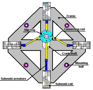 And this is the side view: 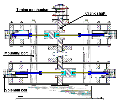 Ben has used eight solenoids to imitate the way that a car engine works. There is a crankshaft and connecting rods, as in any car engine. The connecting rods are connected to a slip-ring on the crankshaft and the solenoids are given a pulse of current at the appropriate moment to pull the crankshaft round. The crankshaft receives four pulls on every revolution. In the arrangement shown here, two solenoids pull at the same moment. In the side view above, each layer has four solenoids and you can extend the crankshaft to have as many layers of four solenoids as you wish. The engine power increases with every layer added. Two layers should be quite adequate as it is a powerful motor with just two layers. An interesting point is that as a solenoid pulse is terminated, its pull is briefly changed to a push due to the weird nature of coils. If the timing of the pulses is just right on this motor, that brief push can be used to increase the power of the motor instead of opposing the motor rotation. This feature is also used in the Adams motor described in the ‘Free-Energy’ section of this document. The strength of the magnetic field produced by the solenoid is affected by the number of turns in the coil, the current flowing through the coil and the nature of what is inside the coil ‘former’ (the tube on which the coil is wound). In passing, there are several fancy ways of winding coils which can also have an effect, but here we will only talk about coils where the turns are wound side by side at right angles to the former.
Transformers Transformers are used to alter the voltage of any alternating current power source. If the alteration increases the output voltage, then the transformer is called a ‘step-up’ transformer. If the output voltage is lower than the input voltage then it is called a ‘step-down’ transformer. If the voltages are the same, it is called an ‘isolation’ transformer. A common construction looks like this: 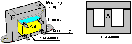 The Coil bobbin sits on the section of the laminations marked ‘A’ above. The coil is wound on its bobbin former, first one winding and then the second winding. The bobbin is then placed on the central part of the ‘E’ shaped laminations and then completely surrounded by the laminations when the crossbar is placed on the top. The mounting strap is used to hold the two sets of laminations together and provide mounting lugs for attaching the transformer to a chassis. There are typically, twenty laminations in each set and every lamination is insulated from the adjoining laminations. If you want to change the voltage of a battery supply, it is possible to build an electronic circuit to generate an alternating voltage and then use a transformer to change that alternating voltage to whatever voltage you want. The most common form of this, is for generating mains voltage from a 12 Volt car battery, so that mains equipment can be run in remote locations, such as boats, caravans, etc. These circuits are called ‘inverters’ and they are very popular pieces of equipment. The voltage in the secondary coil of any transformer is determined by the ratio of the turns in the primary and secondary windings. For example; if there is a 10 Volt alternating voltage available and you have a transformer which has 100 turns in the primary coil and 1000 turns in the secondary coil. If you connect the 10 Volts across the primary, there will be 100 Volts generated across the secondary coil. Instead, if you connect the 10 Volts across the secondary coil, a voltage of 1 Volts will be generated across the primary winding. This is because there is a 10:1 ratio between the two windings. The Law of Conservation of Energy applies to transformers as it does to everything else. The power input to the primary winding will be the same as the power in the secondary winding minus the losses. The losses, in this case, will be a temperature rise of the whole transformer. If the current passed through the transformer is well below its rated capacity, then the losses will be small. The important point is that 10 Volts at 1 Amp into the primary winding will generate 100 Volts in the secondary, but at somewhat less than 0.1 Amps: Power Input is 10 Watts and Power Output is almost 10 Watts. The voltage has been raised to 100 Volts but the potential current draw has been reduced from 1 Amp to 0.1 Amps (100 mA). In practice, the thickness of the wire used in the windings is very important. If the voltage to be placed across the winding is high, then the wire diameter will be small. Coil windings have fairly low resistances but this is not critical in circuits as coils operate in a peculiar way. Coils have AC ‘impedance’ in addition to their DC ‘resistance’. While Direct Current (from a battery, say) can flow quite easily through a coil with low resistance, Alternating Current may have a hard job getting through the coil due to its high ‘impedance’. Sometimes, coils are used to choke off any AC ripple (interference) coming along a DC power cable. When a coil is used for this purpose it is called a ‘choke’. Each coil has its own resonant frequency and at that frequency it is very difficult for AC to get through the coil. Crystal set radios work on that principle: 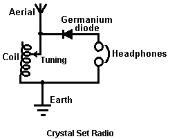 Here, the aerial picks up every radio station broadcasting in the area. These are all at different frequencies and they all head down the aerial wire, looking for the easiest path to the earth connection. Most of them run through the coil with no problem whatsoever. If the resonant frequency of the coil matches the frequency of one of the radio stations, then that radio signal (and only that signal) finds it very hard to get through the coil and looks for an easier path to earth. The next easiest path is through the diode and the headphones, so the signal goes that way. The diode blocks part of the signal which generates the sound of the radio broadcast in the headphones. This system works very well indeed if there is a good radio signal. A germanium diode is used as the radio signal voltage is very small and a germanium diode operates on 0.2 Volts while a silicon diode needs 0.7 Volts to operate. That difference is significant at these very low voltages. The resonant frequency of the coil depends on the number of turns in the coil. In this design, the coil has a slider which allows the number of turns to be altered and so, different radio stations to be tuned in. Rectification and Power Supplies We now have the question of how do we turn an alternating voltage into a constant ‘direct’ voltage. The crystal radio set operates by chopping off half of the alternating radio signal. If we were to do this to the output from a mains transformer with an output of say, 12 Volts AC, the result is not very satisfactory: 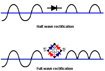 Here, we have the situation shown in the upper diagram. The output consists of isolated pulses at 50 per second. You will notice that there is no output power for half of the time. The negative part of the waveform is blocked by the high resistance of the diode while the positive part of the waveform is allowed through by the low resistance of the ‘forward-biased’ diode. It should be remembered that the diode drops 0.7 Volts when conducting so the output of the half-wave rectified transformer will be 0.7 Volts lower than the transformer’s actual output voltage. If four diodes are used instead of one, they can be arranged as shown in the lower diagram. This arrangement of diodes is called a ‘bridge’. Here the positive part of the waveform flows through the upper blue diode, the load ‘L’ and on through the lower blue diode. The negative part flows through the left hand red diode, the load and then the right hand red diode. This gives a much better output waveform with twice the power available. The output voltage will be 1.4 Volts less than the transformer output voltage as there are two silicon diodes in the supply chain. The output from even the full-wave rectifier is still unsatisfactory as there is a voltage drop to zero volts 100 times per second. Only a few devices operate well with a power supply like that, an incandescent bulb as used in a car can use this output, but then, it could use the original AC supply without any rectification. We need to improve the output by using a reservoir device to supply current during those moments when the voltage drops to zero. The device we need is a Capacitor which used to be called a ‘condenser’. The circuit of a mains unit using a capacitor is shown here: 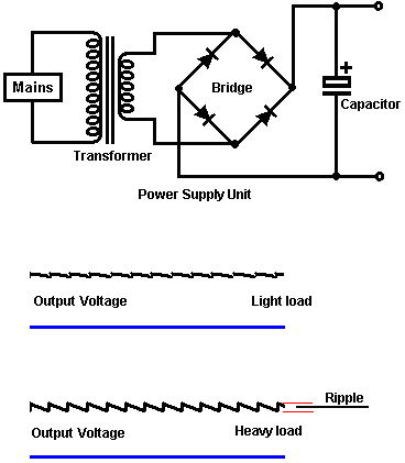 This produces a much better result as the capacitor stores some of the peak energy and gives it out when the voltage drops. If the load on the unit is light with not very much current taken from it, the output voltage is quite good. However, if the current drain is increased, the output voltage gets dragged down 100 times per second. This voltage variation is called ‘ripple’ and if the unit is supplying an audio system or a radio, the ripple may well be heard as an annoying hum. The larger the capacitor for any given current draw, the smaller the ripple. To improve the situation, it is normal to insert an electronic control circuit to oppose the ripple: 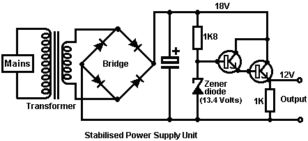 This circuit uses one new component, a new variety of diode called a ‘Zener’ diode. This device has an almost constant voltage drop across it when its current-blocking direction breaks down. The diode is designed to operate in this state to provide a reference voltage. The circuit merely uses a tiny current from the top of the zener diode to drive the Darlington pair emitter-follower transistors used to provide the output current. With this circuit, when the output current is increased, the resistance of the transistor pair automatically reduces to provide more current without varying the output voltage. The 1K resistor is included to give the transistors a completed circuit if no external equipment is connected across the output terminals. The zener diode is chosen to give 1.4 Volts more than the required output voltage as the two transistors drop 1.4 Volts when conducting. You should note that the output transistor is dropping 6 Volts at the full supply current. Watts = Volts x Amps so the power dissipated by the transistor may be quite high. It may well be necessary to mount the transistor on an aluminium plate called a ‘heat sink’ to keep it from overheating. Some power transistors, such as the 2N3055, do not have the case isolated from the active parts of the transistor. It is good practice to use a mica gasket between the transistor and the heat-sink as it conducts then heat without making an electrical connection to the metal heat-sink. A capacitor, being an electrical reservoir, can be used as part of a timer circuit. If the current flow into it is restricted by passing it through a resistor. The length of time between starting the flow on an empty capacitor, and the voltage across the capacitor reaching some chosen level, will be constant for a high-quality capacitor. 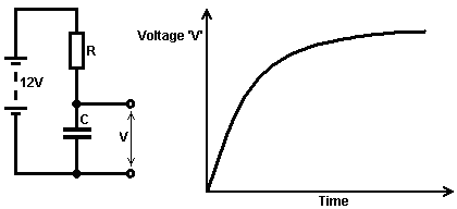 As the voltage increase tails off, it becomes more difficult to measure the difference accurately, so if the capacitor is to be used for generating a time interval, it is normal to use the early part of the graph area where the line is fairly straight and rising fast. The Voltage Doubler It is possible to increase the output voltage of a transformer although this does reduce its ability to supply current at that voltage. The way that this is done is to feed the positive cycles into one storage capacitor and the negative cycles into a second reservoir capacitor. This may sound a little complicated, but in reality, it isn't. A circuit for doing this is shown here: 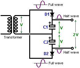 With this circuit, the transformer output is some voltage, say "V" volts of AC current. This output waveform is fed to capacitor "C1" through diode "D1" which lops off the negative part of the cycle. This produces a series of positive half-cycles which charge up capacitor "C1" with a positive voltage of "V". The other half of the output is fed to capacitor "C2" through diode "D2" which cuts off the positive part of the cycle, causing capacitor "C2" to develop a voltage of -V across it. As the two capacitors are 'in series' and not placed across each other, their voltages add up and produce twice the transformer output voltage. A word of warning here. The transformer is producing an AC waveform and these are marked with the average voltage of the waveform, which is usually a sine wave. The peak voltage of a sinewave is 41% greater than this, so if your transformer has an AC output of 10 volts, then the peaks fed to the capacitors will be about 14.1 volts. If there is no current draw from the capacitors (that is, with the load switched off), then each capacitor will charge to this 14.1 volts and the overall output voltage will be 28.2 volts and not the 20 volts which you might expect. You need to understand that as this is only a half-wave supply, there will be considerable ripple on the output voltage if the current draw is high. Using one additional smoothing capacitor and paying attention to the voltage ratings of the capacitors, the 28 volts supply circuit might be like this: 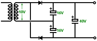 Multivibrators The number of electronic circuits which can be built with basic components such as resistors, capacitors, transistors, coils, etc. is limited only by your imagination and needs. Here is a circuit where two transistors operate as a pair: 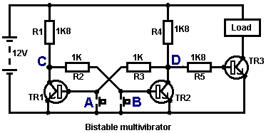 This circuit has two stable states and so it is called a “bi” “stable” or “bistable” circuit. It is important to understand the operation of this simple and useful circuit. If press-button switch ‘A’ is pressed, it short-circuits the base/emitter junction of transistor TR1. This prevents any current flowing in the base/emitter junction and so switches TR1 hard off. This makes the voltage at point ‘C’ rise as high as it can. This leaves transistor TR2 powered by R1 and R2 which have 11.3 Volts across them and switches TR2 hard on. This pulls point ‘D’ down to about 0.1 Volts. This happens in less than a millionth of a second. When the press-button switch ‘A’ is released, transistor TR1 does not switch on again because its base current flows through resistor R3 which is connected to point ‘D’ which is far, far below the 0.7 volts needed to make TR1 start conducting. The result is that when press-button ‘A’ is pressed, transistor TR2 switches on and stays on even when press-button ‘A’ is released. This switches transistor TR3 off and starves the Load of current. This is the first ‘stable state’. The same thing happens when press-button ‘B’ is pressed. This forces transistor TR2 into its ‘off’ state, raising point ‘D’ to a high voltage, switching transistor TR3 hard on, powering the Load and holding transistor TR1 hard off. This is the second of the two ‘stable states’. In effect, this circuit ‘remembers’ which press-button was pressed last, so millions of these circuits are used in computers as Random Access Memory (‘RAM’). The voltage at point ‘C’ is the inverse of the voltage at point ‘D’, so if ‘D’ goes high then ‘C’ goes low and if ‘D’ goes low, then ‘C’ goes high. In passing, the output at ‘D’ is often called ‘Q’ and the output at ‘C’ is called ‘Q-bar’ which is shown as the letter Q with a horizontal line drawn above it. This is shown on the next circuit diagram. A minor variation of this circuit allows a load to be energised when the circuit is powered up: 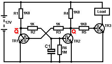 When powered down, the capacitor ‘C1’ in this circuit is fully discharged through resistor ‘R6’. When the 12 Volts supply is connected to the circuit, capacitor C1 does not charge instantly and so holds the base of TR2 down below 0.7 Volts for much longer than it takes for transistor TR1 to switch on (which, in turn, holds TR2 hard off). Mind you, if it is not necessary to have the Load held powered on indefinitely, then an even more simple circuit can do this: 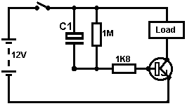 Here, when the switch is closed, both sides of the capacitor C1 are at +12 Volts and this causes the 1K8 resistor to conduct heavily, driving the transistor and powering the load. The capacitor charges rapidly through the transistor and reaches the point at which it can no longer keep the transistor switched on. When the battery is switched off, the 1M resistor discharges the capacitor, ready for the next time the battery is connected. The Monostable Multivibrator. The monostable has one stable state and one unstable state. It can be flipped out of its stable state but it will ‘flop’ back into its stable state. For that reason, it is also known as a ‘flip-flop’ circuit. It is similar to a bistable circuit, but one of the cross-link resistors has been replaced by a capacitor which can pass current like a resistor, but only for a limited amount of time, after which, the capacitor becomes fully charged and the current flow stops, causing the ‘flop’ back to the stable state once more. 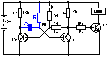 In this circuit, the ‘R’ resistor and the ‘C’ capacitor values determine how long the monostable will be in its unstable state. The circuit operates like this:
The Astable multivibrator. The astable circuit is the monostable with a second capacitor added so that neither state is stable. This results in the circuit flopping backwards and forwards continuously: 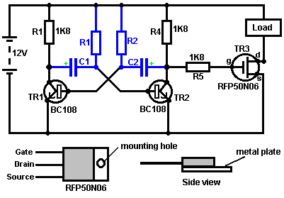 The rate of switching is controlled by the R1/C1 and R2/C2 combinations. The load’s ON time to its OFF time is called the ‘mark-space’ ratio, where the ON period is the ‘mark’ and the OFF period is the ‘space’. If you choose to use electrolytic capacitors which have their own polarity, then the +ve end of each capacitor is connected to the transistor collector. While it is good to understand how these multivibrator circuits operate and can be built, nowadays there are pre-built circuits encased in a single package which you are much more likely to choose to use. These are called Integrated Circuits or ‘ICs’ for short. We will be discussing these shortly. Before we do, notice that in the circuit above, transistor TR3 has been changed to a new variety called a Field Effect Transistor (‘FET’). This type of transistor is newer than the ‘bipolar’ transistors shown in the earlier circuits. FETs come in two varieties: ‘n-channel’ which are like NPN transistors and ‘p-channel’ which are like PNP transistors. FETs are more difficult to make but have now reached a level of cost and reliability which makes them very useful indeed. They require almost no base current (called ‘gate’ current with this type of transistor) which means that they have almost no effect on any circuit to which they are attached. Also, many of them can handle large currents and boast major power handling capabilities. Because of this, it is usual to see them packaged with a metal plate mounting, ready to be bolted to an aluminium heat-sink plate to help dissipate the heat generated by the large amount of power flowing through them. The ‘RFP50N06’ shown above can handle up to 50 Volts and carry up to 60 Amps, which is serious power handling. Inverters Consider the following circuit: 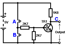 If neither of the press-button switches are operated, the transistor has no base/emitter current flow and so it is off. This places the collector voltage at ‘C’ near the positive rail (+5 Volts). If press-button switch ‘A’ is operated, the base voltage tries to rise to half of the battery voltage but doesn’t make it because the transistor base pins it down to 0.7 Volts. This feeds base current to the transistor, switching it hard on and causing the output at ‘C’ to drop to nearly 0 Volts. If press-button switch ‘B’ is operated (don’t do this when switch ‘A’ is closed or you will get a very high ‘short-circuit’ current flowing directly through the two switches) it has no effect on the output voltage which will stay high. If we re-draw the circuit like this: 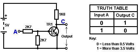 We can see that if the voltage at the input ‘A’ is taken high, then the output voltage at ‘C’ will be low. If the voltage at the input ‘A’ is taken low, then the output voltage at ‘C’ will be high. A circuit which does this is called an ‘Inverter’ because it ‘inverts’ (or ‘turns upside down’) the input voltage. We can summarise this operation in a table. Personally, I would call the table an ‘Input/Output’ table, but for no obvious reason, the standard name is a ‘Truth’ table. The purpose of this table is to list all of the possible inputs and show the corresponding output for each input. Another standard, is to substitute ‘1’ for ‘High Voltage’ and ‘0’ for ‘Low Voltage’. You will notice that many items of electrical and electronic equipment have these symbols on the ON / OFF switch. In computer circuitry (hah! you didn’t notice that we had moved to computer circuits, did you?), the ‘0’ represents any voltage below 0.5 Volts and the ‘1’ represents any voltage above 3.5 Volts. Many, if not most, computers operate their logic circuits on 5 Volts. This Inverter circuit is a ‘logic’ circuit. A criticism of the above circuit is that its input resistance or ‘impedance’ is not particularly high, and its output impedance is not particularly low. We would like our logic circuits to be able to operate the inputs of eight other logic circuits. The jargon for this is that our circuit should have a ‘fan-out’ of eight. Let’s go for a simple modification which will improve the situation: 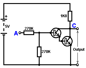 Here, The input impedance has been increased by a factor of 100 by using a Darlington pair of transistors which need far less base current, and so can have a much higher input resistor. Unfortunately, the output impedance is still rather high when the transistors are in their OFF state as any current taken from the positive line has to flow through the 1K8 (1800 ohm) resistor. But we need this resistor for when the transistors are in their ON state. We really need to change the 1K8 resistor for some device which has a high resistance at some times and a low resistance at other times. You probably have not heard of these devices, but they are called ‘transistors’. There are several ways to do this. We might choose to use PNP transistors (we normally use NPN types) and connect these in place of the 1K8 resistor. Perhaps we might use a circuit like this: 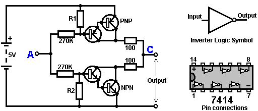 This circuit is starting to look complicated and I don’t like complicated circuits. It is not as bad as it looks. The NPN transistors at the bottom are almost the same as the previous circuit. The only difference is that the collector load is now two 100 ohm resistors plus the resistance of the two transistors. If the PNP transistors are OFF when the NPN transistors are ON, then the circuit loading on the NPN transistors will be negligible and the whole of the NPN transistors output will be available for driving external circuits through the lower 100 ohm resistor (a large ‘fan-out’ for the ‘0’ logic state). To make sure that the PNP transistors are hard off before the NPN transistors start to switch on, the resistor ‘R1’ needs to be selected carefully. The PNP transistors are an exact mirror image of the NPN side, so resistor 'R2' needs to be selected carefully to ensure that the NPN transistors are switched hard OFF before the PNP transistors start to switch ON. You need not concern yourself unduly with that circuit, because you will almost certainly use an Integrated Circuit rather than building your own circuit from ‘discrete’ components. An Integrated Circuit containing six complete inverters is the 7414 which is shown above. This comes in a small black case with two rows of 7 pins which make it look a bit like a caterpillar. Because there are two row of pins, the packaging is called “Dual In-Line” or “DIL” for short. Now, consider the following circuit: 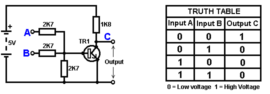 This circuit operates the same way as the Inverter circuit, except that it has two inputs (‘A’ and ‘B’). The output voltage at ‘C’ will be low if either, or both, of the inputs is high. The only time that the output is high, is when both Input ‘A’ AND Input ‘B’ are low. Consequently, the circuit is called an “AND” gate. Strictly speaking, because the output voltage goes Down when the input voltage goes Up, it is called a “not AND” gate, which gets shortened to a “NAND” gate. In this context, the word “not” means “inverted”. If you fed the output ‘C’ into an inverter circuit, the resulting circuit would be a genuine “AND” gate. The digital circuit symbols are: 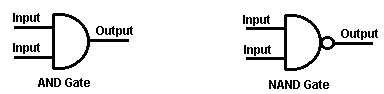 So, why is it called a “Gate” - isn’t it just a double inverter? Well, yes, it is a double inverter, but a double inverter acts as a gate which can pass or block an electronic signal. Consider this circuit: 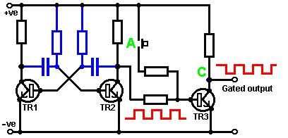 Here, transistors ‘TR1’ and ‘TR2’ are connected to form an astable (multivibrator). The astable runs freely, producing the square wave voltage pattern shown in red. Transistor ‘TR3’ passes this voltage signal on. TR3 inverts the square wave, but this has no practical effect, the output being the same frequency square wave as the signal taken from the collector of TR2. If the press-button switch at point ‘A’ is operated, a current is fed to the base of TR3 which holds it hard on. The voltage at point ‘C’ drops to zero and stays there. The square wave signal coming from the collector of TR2 is blocked and does not reach the output point ‘C’. It is as if a physical ‘gate’ has been closed, blocking the signal from reaching point ‘C’. As long as the voltage at point ‘A’ is low, the gate is open. If the voltage at point ‘A’ goes high, the gate is closed and the output is blocked. There is no need for a manual switch at point ‘A’. Any electronic switching circuit will do: 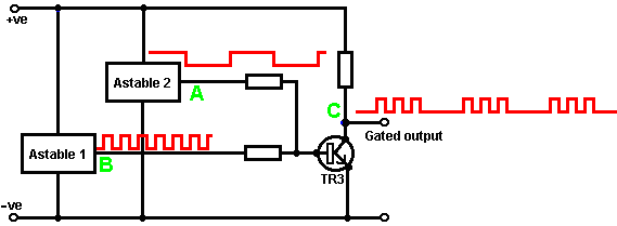 Here, a slow-running astable is substituted for the manual switch. When the output voltage of ‘Astable 2’ goes high, it switches the gate transistor ‘TR3’, holding it hard on and blocking the square-wave signal from ‘Astable 1’. When the output voltage of ‘Astable 2’ goes low, it frees transistor ‘TR3’ and it then passes the ‘Astable 1’ signal through again. The resulting gated waveform is shown in red at point ‘C’ and it is bursts of signal, controlled by the running rate of ‘Astable 2’. This is the sort of waveform which Stan Meyer found very effective in splitting water into Hydrogen and Oxygen (see Chapter 10). This circuit could also be drawn as: 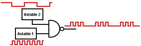 The small circle on the output side of logic devices is to show that they are inverting circuits, in other words, when the input goes up, the output goes down. The two logic devices we have encountered so far have had this circle: the Inverter and the NAND gate. If you wish, you can use a NAND gate chip which has the circuitry also built as a Schmitt trigger, which as you will recall, has a fast-switching output even with a slowly moving input. With a chip like that, you can get three different functions from the one device: 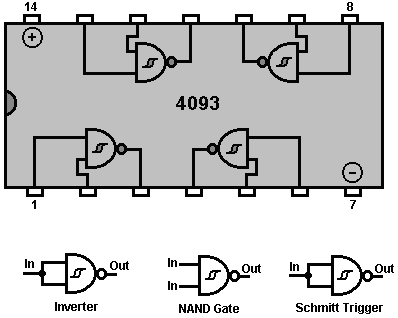 If the two inputs of a NAND gate are connected together, then the output will always be the opposite of the input, i.e. the gate acts as an inverter. This arrangement also works as a Schmitt Trigger due to the way the NAND gate circuitry is built. There are several packages built with this type of circuitry, the one shown here is the “74132” chip which contains four “dual-input” NAND gates. Gates can have almost any number of inputs but it is rare to need more than two in any given circuit. Another chip with identical pin connections is the 4011 chip (which is not a Schmitt circuit). This ‘quad dual-input’ NAND gate package uses a construction method called “CMOS” which is very easily damaged by static electricity until actually connected into a circuit. CMOS chips can use a wide range of voltages and take very little current. They are cheap and very popular The number of devices built into an Integrated Circuit is usually limited by the number of pins in the package and one pin is needed for one connection to ‘the outside world’. Packages are made with 6 pins (typically for opto-isolators), 8 pins (many general circuits), 14 pins (many general circuits, mostly computer logic circuits), 16 pins (ditto, but not as common) and then a jump to large numbers of pins for Large Scale devices such as microprocessors, memory chips, etc. The standard IC package is small:  Prototype circuits are often built on ‘strip board’ which is a stiff board with strips of copper running along one face, and punched with a matrix of holes. The strips are used to make the electrical connections and are broken where necessary. This strip board is usually called “Veroboard”:  Nowadays, the strip board holes are spaced 2.5 mm (1/10”) apart which means that the gaps between the copper strips is very small indeed. I personally, find it quite difficult to make good solder joints on the strips without the solder bridging between two adjacent strips. Probably, a smaller soldering iron is needed. I need to use an 8x magnifying glass to be sure that no solder bridging remains in place before a new circuit is powered up for the first time. Small fingers and good eyesight are a decided advantage for circuit board construction. The narrow spacing of the holes is so that the standard IC DIL package will fit directly on the board. Circuits built using computer circuitry, can experience problems with mechanical switches. An ordinary light switch turns the light on and off. You switch it on and the light comes on. You switch it off and the light goes off. The reason it works so well is that the light bulb takes maybe, a tenth of a second to come on. Computer circuits can switch on and off 100,000 times in that tenth of a second, so some circuits will not work reliably with a mechanical switch. This is because the switch contact bounces when it closes. It may bounce once, twice or several times depending on how the switch is operated. If the switch is being used as an input to a counting circuit, the circuit may count 1, 2 or several switch inputs for one operation of the switch. It is normal to “de-bounce” any mechanical switch. This could be done using a couple of NAND gates connected like this: 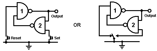 Here, the mechanical switch is buffered by a ‘latch’. When the ‘Set’ switch is operated, the output goes low. The unconnected input of gate ‘1’ acts as if it has a High voltage on it (due to the way the NAND gate circuit was built). The other input is held low by the output of gate ‘2’. This pushes the output of gate ‘1’ high, which in turn, holds the output of gate ‘2’ low. This is the first stable state. When the ‘Set’ switch is operated, the output of gate ‘2’ is driven high. Now, both inputs of gate ‘1’ are high which causes its output to go low. This in turn, drives one input of gate ‘2’ low, which holds the output of gate ‘2’ high. This is the second stable state. To summarise: pressing the ‘Set’ switch any number of times, causes the output to go low, once and only once. The output will stay low until the ‘Reset’ switch is operated once, twice or any number of times, at which point the output will go high and stay there. This circuit uses just half of one cheap NAND gate chip to create a bistable multivibrator which is physically very small and light. Gate Circuits NAND Gates can be used as the heart of many electronic circuits apart from the logic circuits for which the package was designed. Here is a NAND gate version of the rain alarm described earlier. The ‘4011B’ chip is a CMOS device which has a very high input impedance and can operate at convenient battery voltages (3 to 15 Volts): 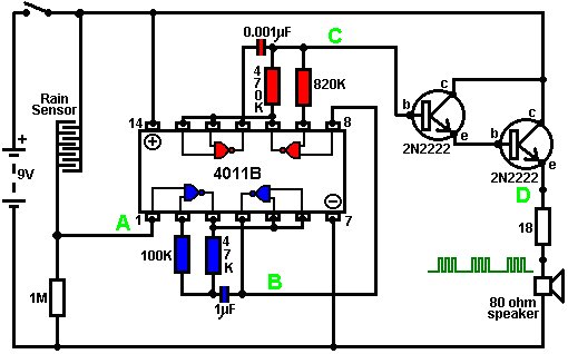 This circuit is comprised of a rain sensor, two astable multivibrators and a power-driver feeding a loudspeaker:
So, why does this circuit oscillate?: 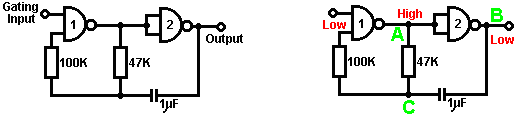 The circuit will not oscillate if the gating input is low, so assume it to be high. Take the moment when the output of gate 2 is low. For this to happen, the inputs of gate 2 have to be high. As the output of gate 1 is wired directly to the inputs of gate 2, it must be high, and for that to be true, at least one of its inputs must be low. This situation is shown on the right. There is now a full voltage drop between point ‘A’ and point ‘B’. The 47K resistor and the capacitor are in series across this voltage drop, so the capacitor starts to charge up, progressively raising the voltage at point ‘C’. The lower the value of the resistor, the faster the voltage rises. The larger the value of the capacitor, the slower the voltage rises. When the voltage at point ‘C’ rises sufficiently, the 100K resistor raises the input voltage of gate 1 far enough to cause it to change state. This creates the following situation: 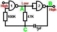 Now, the voltage across ‘A’ to ‘B’ is reversed and the voltage at point ‘C’ starts to fall, its rate governed by the size of the 47K resistor and the 1 microfarad capacitor. When the voltage at point ‘C’ falls low enough, it takes the input of gate 1 low enough (via the 100K resistor) to cause gate 1 to switch state again. This takes the circuit to the initial state discussed. This is why the circuit oscillates continuously until the gating input of gate 1 is taken low to block the oscillation. Now, here is a NAND gate circuit for a sequential on/off switch: 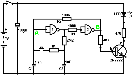 This circuit turns the Light Emitting Diode on and off repeatedly with each operation of the press-button switch. When the on/off switch is closed, capacitor ‘C1’ holds the voltage at point ‘A’ low. This drives the output of gate 1 high, which moves the inputs of gate 2 high via the 100K resistor ‘R1’. This drives the voltage at point ‘B’ low, turning the transistor off, which makes the LED stay in its off state. The low voltage at point ‘B’ is fed back via the 100K resistor ‘R2’ to point ‘A’, keeping it low. This is the first stable state. As the output of gate 1 is high, capacitor ‘C2’ charges up to that voltage via the 2M2 resistor. If the press-button switch is operated briefly, the high voltage of ‘C2’ raises the voltage of point ‘A’, causing gate 1 to change state, and consequently, gate 2 to change state also. Again, the high voltage at point ‘B’ is fed back to point ‘A’ via the 100K resistor ‘R2’, keeping it high, maintaining the situation. This is the second stable state. In this state, point 'B’ has a high voltage and this feeds the base of the transistor via the 4.7K resistor, turning it on and lighting the LED. In this second state, the output of gate 1 is low, so capacitor ‘C2’ discharges rapidly to a low voltage. If the press-button switch is operated again, the low voltage of ‘C2’ drives point ‘A’ low again, causing the circuit to revert to its original stable state. We could, if we wished, modify the circuit so that it would operate for three or four minutes after switch-on but then stop operating until the circuit was turned off and on again. This is accomplished by gating one of the gates instead of just using both as inverters. If we gated the second gate, then the LED would be left permanently on, so we will modify the first gate circuit: 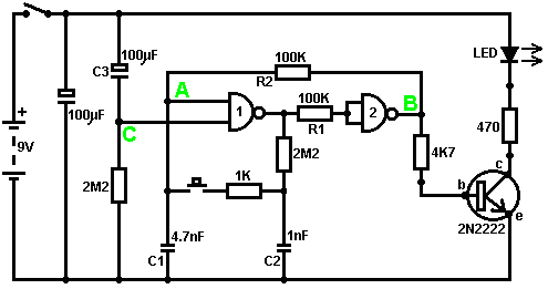 This circuit operates exactly the same way as the previous circuit if, and only if, the voltage at point ‘C’ is high. With the voltage at point ‘C’ high, gate 1 is free to react to the voltage at point ‘A’ as before. If the voltage at point ‘C’ is low, it locks the output of gate 1 at the high level, forcing the output of gate 2 to the low level and holding the LED off. When the circuit is first powered up, the new 100 microfarad capacitor ‘C3’ is fully discharged, which pulls the voltage at point ‘C’ to nearly + 9 Volts. This allows gate 1 to operate freely, and the LED can be toggled on and off as before. As time passes, the charge on capacitor ‘C3’ builds up, fed by the 2M2 resistor. This causes the voltage at point ‘C’ to fall steadily. The rate of fall is governed by the size of the capacitor and the size of the resistor. The larger the resistor, the slower the fall. The larger the capacitor, the slower the fall. The values shown are about as large as are practical, due to the current ‘leakage’ of ‘C3’. After three or four minutes, the voltage at point ‘C’ gets driven low enough to operate gate 1 and prevent further operation of the circuit. This type of circuit could be part of a competitive game where the contestants have a limited time to complete some task. Gates can also be used as amplifiers although they are not intended to be used that way and there are far better integrated circuits from which to build amplifiers. The following circuit shows how this can be done: 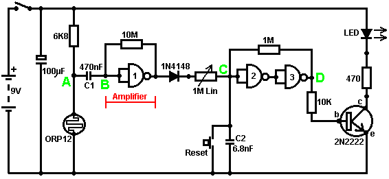 This circuit operates when there is a sudden change in light level. The previous light-level switching circuit was designed to trigger at some particular level of increasing or decreasing level of lighting. This is a shadow-detecting circuit which could be used to detect somebody walking past a light in a corridor or some similar situation. The voltage level at point ‘A’ takes up some value depending on the light level. We are not particularly interested in this voltage level since it is blocked from the following circuitry by capacitor ‘C1’. Point ‘B’ does not get a voltage pulse unless there is a sudden change of voltage at point ‘A’, i.e. there is a sudden change in light level reaching the light-dependent resistor ORP12. The first gate amplifies this pulse by some fifty times. The gate is effectively abused, and forced to operate as an amplifier by the 10M resistor connecting its output to its input. At switch-on, the output of gate 1 tries to go low. As its voltage drops, it starts to take its own inputs down via the resistor. Pushing the voltage on the inputs down, starts to raise the output voltage, which starts to raise the input voltage, which starts to lower the output voltage, which ...... The result is that both the inputs and the output take up some intermediate voltage (which the chip designers did not intend). This intermediate voltage level is easily upset by an external pulse such as that produced by the ORP12 through capacitor ‘C1’. When this pulse arrives, an amplified version of the pulse causes a voltage fluctuation at the output of gate 1. This voltage change is passed through the diode and variable resistor to the input of gate 2. Gates 2 and 3 are wired together as a makeshift Schmitt trigger in that the output voltage at point ‘D’ is fed back to point ‘C’ via a high value resistor. This helps to make their change of state more rapid and decisive. These two gates are used to pass a full change of state to the output stage transistor. The variable resistor is adjusted so that gate 2 is just about to change state and is easily triggered by the pulse from amplifier gate 1. The output is shown as an LED but it can be anything you choose. It could be a relay used to switch on some electrical device, a solenoid used to open a door, a counter to keep track of the number of people using a passageway, etc. etc. Please note that an operational amplifier chip (which will be described later) is a far better choice of IC for a circuit of this type. A gate amplifier is shown here only to show another way that a gate can be utilised. The 'NE555' Timer Chip There is an exceptionally useful chip designated by the number 555. This chip is designed to be used in oscillator and timer circuits. Its use is so widespread that the chip price is very low for its capability. It can operate with voltages from 5 Volts to 18 Volts and its output can handle 200 mA. It takes 1 mA when its output is low and 10 mA when its output is high. It comes in an 8-pin Dual-In-Line package and there is a 14-pin package version which contains two separate 555 circuits. The pin connections are: 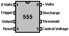 This device can operate as a monostable or astable multivibrator, a Schmitt trigger or an inverting buffer (low current input, high current output). Here it is wired as a Schmitt trigger, and for variation, it is shown triggering a triac which will then stay on until the circuit is powered down (an SCR could be used just as well with this DC circuit): 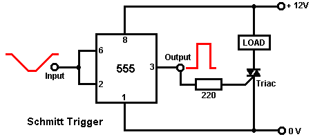 And here, a monostable: 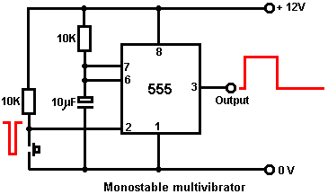 And here are two astables, the second of which has fixed, equal mark/space ratio and the first a high output voltage time determined by Ra + Rb and a low voltage output time determined by Rb (2:1 in this case): 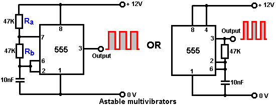 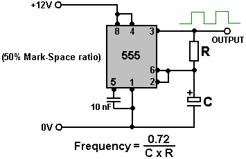  Note: The high leakage of large value electrolytic capacitors prevents them being used with high value resistors in timing circuits. Instead, use a smaller capacitor and follow the timing circuit with a “divide-by-N” chip to give accurately timed long periods. Not all 555 chips have a manufacturing quality sufficient for them to operate reliably above 20,000 Hz, so for the higher frequencies the chip needs to be selected after testing its actual performance. We can also wire the 555 to give a variable mark/space ratio while holding the frequency of the oscillation fixed: 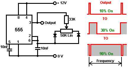 The output waveform changes drastically as the variable resistor is adjusted, but the frequency (or pitch of the note) of the output stays unaltered. A variable-frequency version of this circuit can be produced by changing the 33K resistor to a variable resistor as shown here: 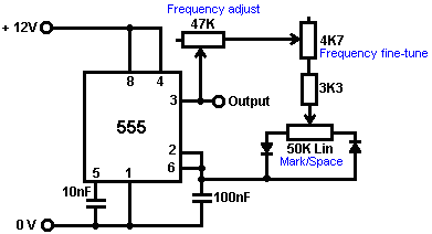 Here, the 33K resistor has been replaced by two variable resistors and one fixed resistor. The main variable resistor is 47K in size (an almost arbitrary choice) and it feeds to a second variable resistor of 4.7K in size. The advantage of this second variable resistor is that it can be set to it’s mid point and the frequency tuning done with the 47K variable. When the frequency is approximately correct, the 4.7K variable can be used to fine tune the frequency. This is convenient as the small variable will have ten times more knob movement compared to the main variable (being just 10% of its value). Obviously, it is not necessary to have the fine-tuning variable resistor, and it can be omitted without changing the operation of the circuit. As the 47K variable resistor can be set to zero resistance and the 4.7K variable resistor can also be set to zero resistance, to avoid a complete short-circuit between output pin 3 and the 50K Mark/Space variable resistor, a 3.3K fixed resistor is included. In this circuit, the frequency is set by your choice of the resistor chain 47K + 4.7K + 3.3K (adjustable from 55K to 3.3K) and the 100nF (0.1 microfarad) capacitor between pin 6 and the zero volt rail. Making the capacitor larger, lowers the frequency range. Making the resistors larger, also lowers the frequency range. Naturally, reducing the size of the capacitor and/or reducing the size of the resistor chain, raises the frequency. One 555 chip can be used to gate a second 555 chip via its pin 4 ‘Reset’ option. You will recall that we have already developed a circuit to do this using two astables and a transistor. We also generated the same effect using four NAND gates. Here, we will create the same output waveform using the more conventional circuitry of two 555 chips: 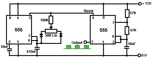 Both of the 555 circuits can be bought in a single 14-pin DIL package which is designated ‘556’. There are many additional circuit types which can be created with the 555 chip. If you wish to explore the possibilities, I suggest that you get a copy of the book “IC 555 Projects” by E.A. Parr, ISBN 0-85934-047-3. A spreadsheet is included which calculates the frequencies produces with various component values for the basic 555 astable and monostable. It also shows the Duty Cycle which is the ratio of the ON time to the OFF time and the actual times of the ON and OFF signals. The “ON” signal is taken to be when the output is at a high voltage. The '741' Chip An important and very useful group of Integrated Circuits is the “Operational Amplifier” or “op-amp” group. These devices have a very high gain, an ‘inverting’ input and a ‘non-inverting’ input. There are many op-amps but we will look at just one popular type called the “741” which has an ‘open-loop’ gain of 100,000 times. All operational amplifiers work in the same way in theory. The way they operate in a circuit is controlled by the external components attached to them. They can operate as inverting amplifier, a non-inverting amplifier (i.e. a ‘buffer’), a comparator, an astable multivibrator, and various other things. The symbol and connections for a 741 op-amp are: 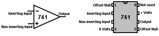 We can connect the 741 chip to act as an amplifier with any set gain level that we choose: 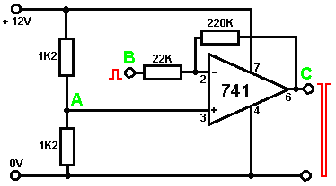 Here, the gain is set by the ratio of the 220K resistor to the 22K resistor. This circuit has a gain of 10 times, so the input signal at point ‘B’ will generate an output signal at point ‘C’ which is ten times larger, provided that the output signal does not approach the battery voltage. If it does, then clipping will occur with the top and the bottom of the output waveform chopped off at about a volt away from the battery voltage levels, approximately 1 Volt and +11 Volts in this example. Operational amplifiers are generally designed to operate from a dual power supply. In the above example, the supply would be created by using two 6 Volts batteries instead of one 12 Volt battery. To avoid the inconvenience of this, a mid-point voltage is generated at point ‘A’ by using two equal resistors in series across the battery. This gives a central voltage of +6 Volts which is fed to the IC. This circuit can be used in many applications. Here is a circuit for a meter to measure sound intensity: 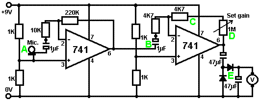 This circuit is two copies of the previous circuit. Each 741 chip has a reference voltage of half the supply voltage created by a voltage-divider pair of 1K resistors. This voltage is fed to pin 3 of the chip, which is the non-inverting input. At point ‘A’, a microphone or small loudspeaker is used to generate a signal voltage when sound reaches it. This voltage is fed to the 741 op-amp via a 1 microfarad blocking capacitor. This passes the audio signal through while blocking the +4.5 Volts DC on pin 3. The first 741 has a gain of 22, set by the 10K and 220K resistors (220/10 = 22). Point ‘B’ then receives an audio signal 22 times larger than the signal produced by the microphone. This signal is still quite small, so the second 741 boosts it further. The gain of the second 741 is variable and depends on the resistance set on the 1M variable resistor. If the variable resistor is set to zero ohms, then the gain of the second 741 will be controlled by the 4K7 resistor at point ‘C’ alone and so will be 1 (4.7/4.7 = 1). If the variable resistor is set to its maximum value, then the gain of the second 741 will be some 214 (1,004,700/4,700 = 213.8). The two op-amps together have a combined gain which ranges from 22 to 4702. The amplified audio signal arrives at point ‘D’ and it can be adjusted to a respectable value. This alternating voltage is now rectified via the diodes at point ‘E’ and it builds up a DC voltage across the 47 microfarad capacitor there. This voltage is displayed on a voltmeter. The result is that the voltmeter shows a reading directly proportional to the sound level reaching the microphone. The 741 can be wired as a buffer. This is the equivalent of an emitter-follower circuit when using transistors. The set up for the 741 is:  Difficult circuit - huh! Are you sure you can afford all the extra components? This circuit utilises the full gain of the 741 chip. The output follows the input waveform exactly. The input requires almost no current, so the circuit is described as having a ‘high input impedance’. The output can drive a serious load such as a relay, so the circuit is described as having a ‘low output impedance’. The 741 chip can be wired to act as a comparator. This is the circuit:  Are you sure you are up to such a difficult circuit? Bit complicated - huh! This is the basic operational form for an operational amplifier. If the voltage at point ‘A’ is higher than the voltage at point ‘B’ then the output goes as low as it can go, say 1 or 2 volts. If the voltage at point ‘A’ is lower than the voltage at point ‘B’ then the output goes as high as it can go, say 10 volts or so. Having seen how transistor circuits work, you should be able to understand why the 741 chip circuitry (which is a transistor circuit inside the 741 package) needs some voltage inside the supply rails to provide an efficient high-current output drive. Here is a 741 version of the light-operated switch: 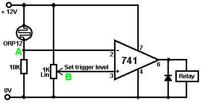 This circuit is set up as evening falls. We want the relay to have minimum voltage across it in daylight, so the voltage at point ‘A’ needs to be higher than the voltage at point ‘B’. As the 1K variable resistor is across the supply voltage, its slider can be set to any voltage between 0 Volts and +12 Volts. To make this easy to do, we choose a ‘linear’ variable resistor as the logarithmic variety would be hard to adjust in this application. With the ‘linear’ version, each 1 degree of rotation of the resistor shaft causes the same change in resistance, anywhere along the range. This is not the case for the logarithmic variety. Anyhow, we adjust the variable resistor downwards until the relay voltage drops to a minimum. When the light level has fallen to the level at which we wish the circuit to trigger, we adjust the variable resistor to make the relay click on. The 741 chip has a very rapid output voltage swing when the input voltages swap over, so the relay switching will be decisive. The switching can be made even more positive by adding a resistor between the output and point ‘B’. This acts like a Schmitt trigger when switching occurs by providing some additional positive feedback, lifting the voltage at point ‘B’. If you wish the circuit to trigger on a rising light level, just swap the positions of the 10K resistor and the ORP12 light-dependent resistor. The same circuit will operate as a temperature sensing circuit by substituting a ‘thermistor’ (which is a temperature-dependent resistor) for the ORP12. If we would like the circuit to act as a burglar alarm, we could use the same circuit like this: 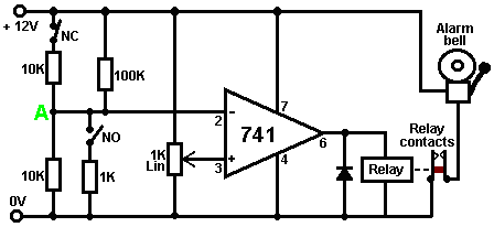 The circuit is still controlled by the voltage at point ‘A’. Under normal circumstances, this voltage will be near +6 Volts (produced by the two 10K resistors and the 100K resistor). The upper switch marked ‘NC’ for ‘Normally Closed’, represents a chain of, say, magnetic switches attached to doors and windows. If any of these are opened, then the voltage at point ‘A’ will be dictated by the lower 10K resistor in series with the 100K resistor. This will cause the voltage at ‘A’ to fall instantly to a low value, triggering the circuit. The ‘NO’ switch (‘Normally Open’) represents one or more pressure-operated switches under carpets or rugs and/or switches which get brushed when doors are swung open, etc. These switches are wired in parallel across each other and if any of them is closed for even a millionth of a second, the voltage at point ’A’ will be pulled down by the 1K resistor and the circuit will be triggered. The circuit can be latched on in any one of a variety of ways. One relay contact can be used to hold the relay on or hold the voltage at ‘A’ low. A transistor can be wired across the relay to hold the circuit on, etc. etc. If this is done, the circuit will remain in its triggered state until the supply voltage is interrupted. You might prefer to use a 555 chip to limit the length of time the alarm sounds to three minutes or so. An alternative to using a relay or semiconductor latch is to use a Silicon Controlled Rectifier usually referred to as an ‘SCR’ or ‘Thyristor’. This device is normally “off” with a very high resistance to current flow. If it is switched on by applying a voltage to its Gate connection, it stays continuously on until some external device stops current flowing through it. The following circuit shows how it operates:  When the voltage is first applied to the circuit by closing switch S2, the SCR is in its OFF state so no current is supplied to the load. If the press-button switch S1 is pressed, a current is fed into the Gate of the SCR, turning it ON. When switch S1 is allowed to open, the SCR remains in its ON state and it will stay that way until the current through it is cut off. Opening switch S2 cuts off the current to the load and the SCR returns to its OFF state. A very valid question would be: “Why have an SCR at all and just turn the load on and off with switch S2?”. The answer is that switch S1 might be the under-carpet pressure pad of a burglar-alarm and it might be operated some hours after switch S2 was closed to activate the alarm system. Stepping off the pressure pad does not stop the alarm sounding. While this sort of DC latching action is useful, it is more common for an SCR to be used in an AC circuit. For example, take the circuit shown here: 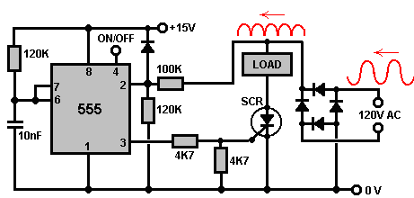 The 120 volt AC supply coming in from the right hand side, is converted to positive-going sine-wave pulses by the diode bridge. This pulsing voltage is applied to the Load/SCR path. If the voltage at pin 3 of the 555 chip is low, then the SCR will remain OFF and no current will be fed to the load device. If the voltage on pin 3 goes high and the voltage applied to the Load/SCR chain is high, then the SCR will be switched ON, powering the load until the pulsing voltage drops to its zero level again some 1/120 of a second later. The 555 chip is connected to form a monostable multivibrator and the timing components (the 120K resistor and the 10nF capacitor) cause it to output a 1 millisecond pulse which is long enough to trigger the SCR into its ON state, but short enough to have finished before the mains pulse reaches its zero-voltage level again. The 555 chip is triggered by the rising mains voltage being passed to its pin 2 through the voltage-divider 100K and 120K pair of resistors, and that synchronises it with the AC waveform. Pin 4 of the 555 chip can be used to switch the load power on and off. In the circuit shown above, the diode bridge is needed to convert the incoming AC waveform to pulsing DC as shown in red in the diagram, as the SCR can only handle current flowing in one direction. The AC load equipment works just as well with the pulsing DC as with a full blown AC waveform. A better semiconductor construction is the ‘Triac’ which acts like two SCR devices back-to-back in a single package. It is shown like this in circuit diagrams: 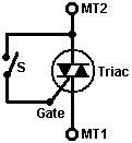 There are three connections to the device: Main Terminal 1, Main Terminal 2 and the Gate. When switch ‘S’ shown in the diagram is closed, the triac conducts on both positive and negative voltages applied to its MT1 and MT2 terminals. When the switch is open, the device does not conduct at all. If the external circuit containing switch ‘S’ is placed inside the device as a permanently closed circuit, then the device becomes a ‘Diac’ which can be used to trigger a Triac and give a very neat circuit for controlling the power to an item of AC mains equipment as shown here: 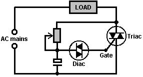 Here, the variable resistor/capacitor pair controls the point on the AC waveform that the Triac is triggered and so controls how much of each sinewave cycle is passed to the mains equipment, and so it controls the average power passed to the equipment. A very common use for a circuit of this type is the ‘dimmer-switch’ used with household lighting. To return now to the 741 chip. The 741 can also be used as an astable multivibrator. The circuit is: 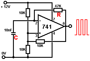 The rate of oscillation of this circuit is governed by the Resistor marked ‘R’ in the diagram and the capacitor marked ‘C’. The larger the resistor, the lower the rate of oscillation, the larger the capacitor, the lower the rate of oscillation. When the output goes high, capacitor ‘C’ charges up until the voltage on it exceeds the mid-rail voltage on pin 3, at which time the 741 output goes low. The capacitor now discharges through resistor ‘R’ until the voltage on it drops below the voltage on pin 3, at which time the output goes high again. The 10K resistor connecting the output to pin 3 provides some positive feedback which makes the 741 act quite like a Schmitt trigger, sharpening up the switching. The same arrangement of resistor and capacitor applied to a Schmitt inverter or Schmitt NAND gate causes exactly the same oscillation: 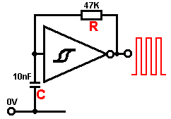 If you would like to see additional ways of using 741 and 555 chips, I can recommend the excellent book “Elementary Electronics” by Mel Sladdin and Alan Johnson ISBN 0 340 51373 X. The '4022' Chip One very useful CMOS integrated circuit is the ‘4022’ chip which is a 16-pin ‘divide by 8’ chip with built-in decoding. The connections are:  If pin 14 is provided with the output from some variety of astable multivibrator, on the first pulse, this chip sets the “0” output on pin 2 to High while the other outputs are Low. On the next pulse, the “0” output goes Low and the “1” output on pin 1 goes High. On the next pulse, output “1” goes Low and the “2” output on pin 3, goes High. And so on until on the eighth pulse, output “7” on pin 10 goes Low and output “0” goes high again. The chip can also divide by lower numbers: For ‘Divide by 7’ operation, connect pin 10 to pin 15 (this resets the output to ‘0’) For ‘Divide by 6’ operation, connect pin 5 to pin 15 For ‘Divide by 5’ operation, connect pin 4 to pin 15 For ‘Divide by 4’ operation, connect pin 11 to pin 15 For ‘Divide by 3’ operation, connect pin 7 to pin 15 For ‘Divide by 2’ operation, connect pin 3 to pin 15 If you want a ‘Divide by 1’ circuit, I suggest you cut down on the amount of alcohol you drink. Here is an illustration of a ‘Divide by 4’ setup: 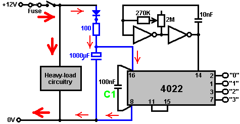 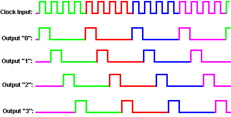 There are a number of things to notice in the above diagram. Firstly, the practical arrangements for circuitry have not been stressed before. If the circuitry has a pulsing circuit drawing heavy current, as shown by the thick red arrows, then it should be physically connected to the battery and any low-current circuitry should be further away from the battery. The supply from the battery should have a fuse or circuit breaker and a switch in the line before anything else is connected, so that if any component develops a fault and goes short-circuit, the fuse will blow and prevent any significant problems. Secondly, it is a good idea to provide the other circuitry with a smoothed power supply as shown by the blue components in the diagram. This minimises the effect if the battery voltage gets pulled down by the pulsing of the high-current circuitry. The diode (silicon, 1 Amp, 50 V) stops the heavy current circuit drawing current from the large smoothing capacitor. The 100 ohm resistor limits the current into the large capacitor on switch-on and provides a little more smoothing. This circuitry is called “de-coupling” as it de-couples the low current circuitry from the high current circuitry. Thirdly, notice capacitor “C1” which is wired physically as close to the power supply pins of the integrated circuit as is possible. If a spike is superimposed on the battery supply, then this capacitor soaks it up and prevents it damaging or triggering the integrated circuit. A spike could be caused by a very strong magnetic pulse nearby as that can induce an extra voltage in the battery wires. The lower part of the diagram shows the output voltages produced as the clock pulses reach pin 14 of the chip. The positive-going part of the clock signal triggers the change in state of the outputs. If necessary, a positive-going pulse on the reset pin, pin 15, causes output “0” to go high and the other outputs to go low. Capacitors We have avoided mentioning capacitors in any detail as it has not been necessary for understanding the circuitry covered so far. Capacitors come in many sizes, types and makes. Their size is stated in ‘Farads’ but as the Farad is a very large unit, you are unlikely to encounter a capacitor marked in anything larger than a microfarad, which is a millionth of a Farad. The symbol for a microfarad is mu-F where ‘mu’ is the letter of the Greek alphabet. This is a pain for normal text production as Greek letters do not occur in your average font. Some circuit diagrams give up on ‘mu’ and just write it as uF which looks like mu-F slightly mis-printed where the descender of the mu has not printed. Anyway, very large capacitors which you may encounter range from 5,000 microfarads to maybe as much as 20,000 microfarads. Large capacitors range from 10 microfarads to 5000 microfarads. Medium sized capacitors run from 0.1 microfarad to about 5 microfarads and small capacitors are those below 0.1 microfarad. 1000 nanofarads (‘nF’) = 1 microfarad. 1000 picofarads (‘pF’) = 1 nanofarad So: 0.01 microfarad can be written as 10nF 0.1 microfarad can be written as 100nF 0.1nF can be written as 100pF Capacitors larger than 1 microfarad tend to be ‘polarised’. In other words, the capacitor has a ‘+’ connector and a ‘-’ connector, and it does matter which way round you connect it. The larger capacitors have a voltage rating and this should not be exceeded as the capacitor can be damaged and possibly even totally destroyed. Capacitors can be added together, but surprisingly, they add in the reverse way to resistors:  If two capacitors are wired in series, as shown in Example 1 above, the overall capacity is reduced while the voltage rating increases. The reduction in capacitance is given by: 1/Ct = 1/C1 + 1/C2 + 1/C3 + ..... In Example 1, then, 1 / total capacitance = 1 / 100 + 1 / 100 or 1 / Ct = 2 / 100 or 1 / Ct = 1 / 50 so the overall capacitance reduces from 100 microfarads to 50 microfarads. The advantage in wiring the capacitors like this is that the voltage rating has now increased to 32V (16V across each of the capacitors). In Example 2, the overall capacitance has reduced to a third of 100 microfarads but the voltage rating has tripled. In Example 3, the capacitors are wired in parallel. The voltage rating is unchanged but the overall capacitance is now the sum of the three capacitors, namely 300 microfarads. There is no need for the capacitors to have similar values, there are merely shown that way in the examples to make the arithmetic easier and not distract you from the ways in which the capacitors interact together. Occasionally, a circuit needs a large capacitor which is not polarised. This can be provided by placing two polarised capacitors back-to back like this: 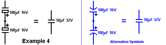 When the capacitors are connected this way, it does not matter which end of the pair is connected to the positive side of the circuit and which to the negative side. The time has come for a serious warning: High voltages are very, very dangerous. Do not become so familiar with them that you treat them casually. High voltages can kill you. Capacitors are capable of building up high voltages and some good makes can hold the charge for several days. In particular, do not try to make adjustments to, or take parts from, the inside of a TV set. A black and white TV set uses 18,000 Volts on the magnetic coils used to create the moving picture on the tube. A capacitor inside the set may well have that voltage on it three days after the set was last used. Don’t fool around inside a TV set, it could kill you quick, or if you are really unlucky, it could injure you for life. A colour TV set uses 27,000 Volts to operate the coils inside it and that will fry you in jig time if you touch it. Also, please don’t think that you are safe if you don’t quite touch it; 27,000 volts can jump across a gap to your hand. If you try to discharge a TV capacitor using a metal screwdriver with a wooden handle, please ensure that you medical insurance is up to date before you do it. You can receive a hefty shock through the screwdriver handle. Voltages up to 24 Volts should be quite safe. However, some circuits will generate very high voltages even though the battery driving the circuit is low voltage. A standard off-the-shelf inverter circuit produces 240 Volts AC from a 12 Volt battery. Just because the battery is only 12 Volts does not mean that the circuit is not dangerous. Circuits which have inductors in them can produce high voltages, especially if they contain large capacitors. The voltage which produces the spark in your car engine is very high and it comes from the 12-volt car battery. You know enough about this by now, so pay attention! Prototype Construction The main options for building a prototype circuit are: 1. A breadboard 2. Electrical screw connector strips. 3. Stripboard 4. A printed circuit board. 1. The typical breadboard unit consists of a matrix of clip holes wired in strips, into which component leads can be pushed to make a circuit. In my opinion, they are best avoided as it takes quite some effort to implement any significant circuit using them, some components do not fit well in the sockets which are small enough to take DIL IC packages, and when you do get a circuit working well on the breadboard, there is no guarantee that it will work well when you attempt to move it to a permanent soldered board: 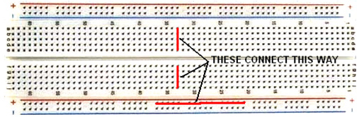 While a plastic board of this type looks as if it should be quick and easy to use, I have never found it to be so ever since the boards were scaled down in size to take the closely-spaced pins of integrated circuits ("chips"). It is generally difficult to lay the components out in the same pattern as the circuit diagram, and if they are not, then it becomes slow to follow the circuit through on the breadboard layout. 2. The local hardware shop has cheap screw connectors which can be very effective. These come in several sizes and the smaller ones are very convenient for constructing transistor circuitry. They look like this:  Circuits can be assembled very easily, using these connectors and an example might be one of the John Bedini battery pulsing circuits which might have a layout like this: 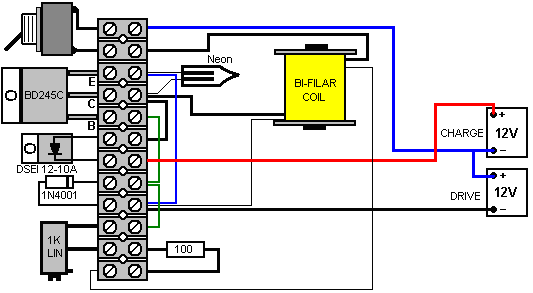 I have built this circuit using this style of construction and it was very successful indeed, being very quick and easy to construct and it proved to be very tough and effective over a long period of use. The plastic strip has a hole between each connector strip and that allows you to bolt the strip to a base board on which you mount other components, in this case, the pulsing coil and the rotor with the magnets attached. Each connection block can take two or three wires. The wires need to have the insulation removed and the wires scraped clean and shiny if they are not already in that state. If more than one multi-strand wire is being put into one side of a connector, then it is usually best to twist the wires together before tightening the clamping screw. If you want, you can give the twisted wires a thin coat of solder, but this has to be done neatly to avoid producing a joint which is too large to fit into the connector. One connector can be cut out of the strip quite easily, using a pair of scissors or a craft knife. Single connectors can join two wires very effectively without the need to solder them. 3. Stripboard, usually called ‘Veroboard’ even if it is not made by Vero, is a quick and satisfactory method, although you have to make very tiny solder joints. Please be aware that the fumes from the burning resin when soldering are most definitely not good for your health and should be avoided by making sure that the ventilation is adequate. 4. A printed circuit board is feasible for a one-off prototype and making one will increase your production skills, so it is also a reasonable option if you have the etching and drilling equipment to hand. Buying all of the necessary equipment if you do not have any, can cost a fair amount, but the skills gained are significant and the finished boards looks very professional. There are several other methods of construction, and many varieties of construction board and stripboard. Simple stripboard will be used in the following descriptions, although the method does apply to many different styles of construction. The first step is to produce a layout for the components on the board. When designing the layout provision should be made for drilling holes to allow the completed board to be bolted to its case using bolts and insulating pillars to keep the soldered joints clear of all other surfaces. 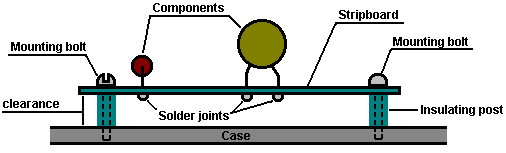 The circuit diagram of the circuit to be built is the starting point. You might wish to draw a light grid of lines to represent the matrix of holes in the strip board. This helps to visualise the run of the copper strips and the sketch can be made to show the exact number of holes available on the piece of strip board to be used. The strip board looks like this: So you might wish to produce a layout sketch re-usable drawing like this:  where the horizontal strips are numbered and the vertical lines of holes are also numbered. In this sketch, where the lines cross, represents a hole in the board. The sketch of a possible physical layout can then be prepared and it might look like this when seen from the top although the copper strips on the underside of the board are shown in the sketch: 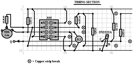 It is very important when producing a sketch like this, that the copper strips making up the circuit are not accidentally used to connect components further along the board, without breaking the copper strip between the two sections of the board. It helps to mark a copy of the circuit diagram when you are sketching a possible physical layout on the strip board. It might be done like this: 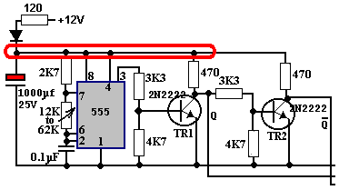 Here, the components just below the diode are ringed to show that they have been marked on the layout sketch and, if necessary, the copper strip broken to isolate the components. A component worth mentioning in passing, is the capacitor marked with red in the circuit diagram. This is a decoupling capacitor, fed from the 12V battery via a resistor and a diode (a diode is not normally used in this part of the circuit). The decoupling is to provide the 555 chip and drivers with a supply which is reasonably isolated from the heavy current-draw circuit not shown in this small section of the circuit diagram. The pulsating heavy current draw of the rest of the circuit is capable of pulling the battery voltage down slightly many times per second. This creates a voltage ripple on the positive supply line from the battery and to smother the ripple, the resistor and diode are used to feed a large reservoir capacitor which smoothes out the ripple. The circuit itself is not beyond criticism. Transistor ‘TR2’ and its associated components are redundant since pin 3 of the 555 chip already supplies the required signal (and with higher drive capacity) so the second output line should be taken directly from pin 3 of the 555 chip. This snippet of circuit is only shown here as an example of marking up a circuit diagram when making a components layout sketch. As the layout sketch is produced, the circuit diagram should be marked off with a highlighting pen to make sure that every part of the circuit diagram has been successfully copied to the sketch. In the example below, not all of the highlighted strip is shown, since it runs off the small section of the board being shown here: 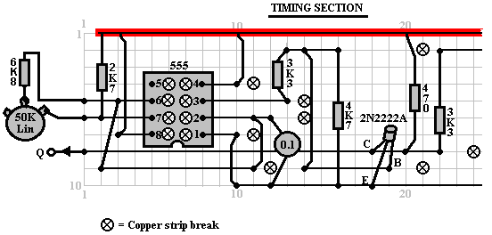 Many electronic components can be damaged by the high temperatures they are subjected to when being soldered in place. I personally prefer to use a pair of long-nosed pliers to grip the component leads on the upper side of the board while making the solder joint on the underside of the board. The heat running up the component lead then gets diverted into the large volume of metal in the pair of pliers and the component is protected from excessive heat. On the same principle, I always use a DIL socket when soldering a circuit board, that way, the heat has dissipated fully before the IC is plugged into the socket. It also has the advantage that the IC can be replaced without any difficulty should it become damaged. If you are using CMOS integrated circuits in any construction, you need to avoid static electricity. Very high levels of voltage build up on your clothes through brushing against objects. This voltage is in the thousands of volts range. It can supply so little current that it does not bother you and you probably do not notice it. CMOS devices operate on such low amounts of current that they can very easily be damaged by your static electricity. Computer hardware professionals wear an earthing lead strapped to their wrists when handling CMOS circuitry. There is no need for you to go that far. CMOS devices are supplied with their leads embedded in a conducting material. Leave them in the material until you are ready to plug them into the circuit and then only hold the plastic body of the case and do not touch any of the pins. Once in place in the circuit, the circuit components will prevent the build up of static charges on the chip. Soldering is an easily-acquired skill. Multi-cored solder is used for electronic circuit soldering. This solder wire has flux resin contained within it and when melted on a metal surface, the flux removes the oxide layer on the metal, allowing a proper electrical joint to be made. Consequently, it is important that the solder is placed on the joint area and the soldering iron placed on it when it is already in position. If this is done, the flux can clean the joint area and the joint will be good. If the solder is placed on the soldering iron and then the iron moved to the joint, the flux will have burnt away before the joint area is reached and the resulting joint will not be good. A good solder joint will have a smooth shiny surface and pulling any wire going into the joint will have no effect as the wire is now solidly incorporated into the joint. Making a good solder joint takes about half a second and certainly not more than one second. You want to remove the soldering iron from the joint before an excessive amount of heat is run into the joint. It is recommended that a good mechanical joint be made before soldering when connecting a wire to some form of terminal (this is often not possible). The technique which I use is to stand the solder up on the workbench and bend the end so that it is sloping downwards towards me. The lead of the component to be soldered is placed in the hole in the strip board and gripped just above the board with long-nosed pliers. The board is turned upside down and the left thumb used to clamp the board against the pliers. The board and pliers are then moved underneath the solder and positioned so that the solder lies on the copper strip, touching the component lead. The right hand is now used to place the soldering iron briefly on the solder. This melts the solder on the joint, allowing the flux to clean the area and producing a good joint. After the joint is made, the board is still held with the pliers until the joint has cooled down. Test Equipment When developing new circuitry, it may be convenient to try different values of resistor in some position in the circuit (the resistor value may be dependent on the gain of a transistor or the actual resistance of an ORP12, or some such other situation). For this, it is very convenient to have a resistor-substitution box which allows you to select any standard resistor at the turn of a switch. These are not readily available on the market. In years gone by, it was possible to buy custom wafer switches, where the number of wafers could be built up to whatever switch size was required, but these do not seem to be available any more. A slightly less convenient method of construction is to use four of these, selected by a second wafer switch: 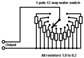 In the above diagram, all of the resistors in one range (100 ohms to 820 ohms, 1K to 8K2, 10K to 82K or 100K to 820K) are wired to a single 12-way switch. The output wires then have any of these standard resistors across them, depending on the setting of the switch. A second switch can then be used to select several of these groups, while still using the same output wires. When boxed, it might look like this: 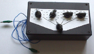 It can also be useful to have a versatile signal generator. You can easily construct your own with variable frequency, variable mark/space ratio and optional variable gating. If you do, you might as well make it with a low output impedance so that it can drive devices under test directly rather than having to provide additional buffering. It might look like this: 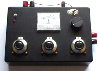 The really essential item of equipment is a multimeter. These come in many shapes, sizes and varieties and the cost varies enormously. The reliability also varies a great deal. The most reliable and the cheapest is the analogue type which does not use a battery (other than for the occasional measurement of resistance). Although these types are looked down upon nowadays, they are 100% reliable: 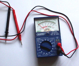 The meter shown above is rated at 2,000 ohms per volt, so connecting it to a circuit to make a measurement on the 10V range is the same as connecting a 20K resistor to the circuit. The big brother of this style of equipment is about five times larger and has 30,000 ohms per volt performance, so connecting it on a 10V range is the same as connecting a 300K resistor to the circuit being measured. This one is battery driven, so if you get one of these, may I suggest that you check its accuracy on a regular basis: 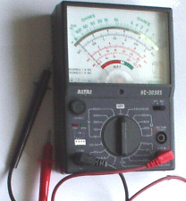 The really excellent non-battery (ex-professional) Avo meter multimeters are still available through eBay at affordable prices. These have 30,000 ohms per volt performance and are robust and accurate, having been built to very high standards. A multimeter uses a 1.5V battery to measure resistance. Ohm’s Law is used as the working principle and the operation is: 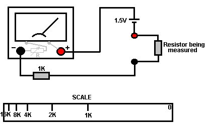 The meter shown in the diagram has a small resistance of its own. This has a small variable resistor added to it. This variable resistor will have a small knob mounted on the face of the multimeter, or it will be a thumbwheel knob projecting slightly from the right hand side of the multimeter case. The 1.5V battery will be positioned inside the multimeter case as is the 1K resistor. To use the resistance ranges, the multimeter probes are touched firmly together to form a short-circuit and the variable resistor adjusted so that the meter points to zero. For the purpose of this discussion, let us assume that the internal resistance of the meter, when correctly adjusted, is exactly 1K. If the resistor under test is exactly 1K in value, then the current through the meter will be halved and the meter will show a needle deflection half way across the scale. If the resistor under test is 2K, then the current will be one third and the scale marking will be at the 1/3 position from the left. If the resistor is 4K, then there will be one fifth (1K+4K=5K) of the full-scale current and the 4K mark will be 20% from the left hand side of the scale. Two things to notice: firstly, the scale has to read from right to left which can take some getting used to, and secondly, the scale is not linear, with the markings getting closer and closer together and consequently, more difficult to mark and read, the higher the value of the resistor being measured. The bunching up of the scale markings is why the more expensive multimeters tend to have more than one range. A mains-operated oscilloscope is an excellent piece of equipment to own but they are expensive when new. It is possible to pick one up at a reasonable price second-hand via eBay. An oscilloscope is by no means an essential item of equipment. One of its most useful features is the ability to measure the frequency, and display the shape of a waveform. Most waveforms are of known shape so the frequency is the major unknown. The following meter is not expensive and it displays the frequency of a signal on a digital readout: 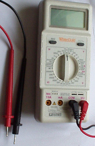 So, when you are deciding what multimeter to buy, consider the following points:
Look around and see what is available, how much it costs and what appeals to you. It might not be a bad idea to buy a really cheap multimeter and use it for a while to see if it has any shortcomings which are a nuisance, and if so, what improvements you personally want from a more expensive meter. It might be worth getting a fancy bench power supply which allows you to set any voltage you want and which displays the current being drawn by your development circuit: 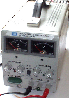 However, there is no need to spend money on a fancy unit when you can build an excellent unit of your own with voltage stabilisation, adjustable output, metered current, etc. etc. Personally, if developing a circuit to be used with a battery, I believe you are better off powering the development from a battery, that way the characteristics of the battery are included in any tests which you carry out. Power Supply: If you wish, you can construct a very convenient development test bed power supply system. This has the advantage that you can make it in the most convenient style for your own use. You can also make the protection ultra-sensitive and build in additional circuitry such as transistor tester and resistor substitution box to produce an integrated test bed. You could perhaps use a circuit like this: 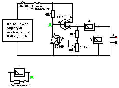 Here, the power is supplied by a pack of re-chargeable Ni-Cad batteries or possibly, a mains unit with voltage stabilisation. As in all actual circuits, the next thing in the circuit is always an on/off switch so that the power source can be disconnected immediately should any problem arise. Next, as always, comes a fuse or circuit breaker, so that should the problem be serious, it can disconnect the circuit faster than you can react. If you wish, you can build your own super-accurate adjustable circuit breaker to use in this position. The two transistors and three resistors form an adjustable, stabilised output. The FET transistor has a high output power handling capacity and a very low input power requirement and so is good for controlling the output voltage. Resistor ‘VR1’ is padded with the 4K7 resistor solely to reduce the voltage across the variable resistor. VR1 is adjusted to control the output voltage. If the current draw is increased and the output voltage is pulled down slightly, then the voltage on the base of the BC109 transistor is reduced. This starts to turn the transistor off, raising the voltage at point ‘A’, which in turn, raises the output voltage, opposing the variation caused by the load. The output is monitored, firstly by a large milliammeter to show the current draw and secondly, on the output side of the milliammeter, a voltmeter. This allows very close monitoring of the power supplied to the prototype, especially if the milliammeter is placed alongside the prototype. You can build this circuit into a wide flat box which provides a working surface beside the milliammeter. At point ‘B’ in the above diagram, a method for altering the current range of the milliammeter by placing a ‘shunt’ resistor across it. When the switch is closed, some current flows through the resistor and some through the milliammeter. This resistor has a very low value, so you are better off making it yourself. Let’s say we wish to double the range of the meter. Solder the switch across the meter and for the resistor use a length of enamelled copper wire wound around a small former. Put a load on the output so that the meter shows a full-scale deflection. Close the switch. If the current displayed is exactly half of what it was, if not, switch off, remove some wire to lower the reading or add some wire to raise the reading and repeat the test until exactly half the current is displayed. The lower the value of the shunt resistor, the more current flows through it and the less through the meter, which then gives a lower reading. Please note: it is very important to have a fuse or circuit breaker in the power being delivered to your test circuit. Any error in building the prototype can cause a major current to be drawn from the supply and this can be dangerous. Remember, you can’t see the current. Even if you have a meter on the current being delivered, you may not notice the high reading. The first sign of trouble may be smoke! You can easily fry the circuit you are building if you do not have a safety cut-off, so use a fuse or other device which limits the current to twice what you are expecting the circuit to draw. So, after all that, what equipment do you really need? You need a small soldering iron and multicore solder, a pair of long-nosed pliers and a multimeter. One other thing is some tool to cut wires and remove the insulation prior to soldering. Personal preferences vary. Some people prefer one of the many custom tools, some people use a knife, I personally use a pair of straight nail scissors. You pick whatever you are comfortable with. Not exactly a vast array of essential equipment. The other items mentioned are not by any means essential so I suggest that you start by keeping things simple and use a minimum of gear. If you are not familiar with electronics, I suggest that you get a copy of the Maplin catalogue, either from one of their shops or via the Maplin web site. Go through it carefully as it will show you what components are available, how much they cost and often, how they are used. The specifications of almost any semiconductor can be found free at AllDataSheet in the form of an Adobe Acrobat document. Finally, because it is not important, all of the circuitry shown so far has indicated current flowing from the + of a battery to the - terminal. The discovery of voltage was made by Volta but he had no way of knowing which way the current was flowing, so he guessed. He had a 50 - 50 chance of getting it right but he was not lucky and got it wrong. Electrical current is actually a flow of electrons, and these flow from the battery minus to the battery plus. So, who cares? Almost nobody, as it has no practical effect on any of the circuitry. Some useful websites: E.S.R. for components Maplin for components AllDataSheet for semiconductor specifications Cricklewood Electronics for components Greenweld for components The Oscilloscope: If you do decide that you are going to research new equipment, design and possibly invent new devices, then an oscilloscope is useful. Let me stress again that this is not an essential item of equipment and most certainly is not needed until you are quite familiar with constructing prototypes. It is quite easy to misread the settings of an oscilloscope and the methods of operation take some getting used to. The low-cost book “How to Use Oscilloscopes and Other Test Equipment” by R.A. Penfold, ISBN 0 85934 212 3 might well be helpful when starting to use a ‘scope. It is possible to get an oscilloscope at reasonable cost by buying second-hand through eBay. The best scopes are ‘dual trace’ which means that they can display the input waveform and the output waveform on screen at the same time. This is a very useful feature, but because it is, the scope which have that facility sell at higher prices. The higher the frequency which the scope can handle, the more useful it is, but again, the higher the selling price. Not all scopes are supplied with (the essential) ‘test probes’, so it might be necessary to buy them separately if the seller wants to keep his. Getting the manual for the scope is also a decided plus. A low cost scope might look like this:  Magnetic Measurement. People who experiment with permanent magnets, can make use of an instrument which displays the strength of a magnetic field. Professionally made devices to do this tend to be well outside the purchasing power of the average experimenter who will already have spent money on materials for his prototypes. Here is a design for a simple and cheap circuit, powered by four AA dry cell batteries, and utilising a Hall-effect semiconductor as the sensor:   This design uses an OP77GP operational amplifier chip to boost the output signal from the A1302 chip which is a Hall-effect device. The gain of the DC-connected operational amplifier is set by the ratio of the 1K and 1M fixed resistors shown shaded in the circuit diagram, giving a gain of 1,000. The circuit operation is simple. The six-volt battery charges the 10 microfarad capacitor which helps iron out any supply line fluctuations caused by varying current draw by the circuit. The 10K variable resistor is used to set the output meter display to zero when the Hall-effect device is not near any magnet. The 1K variable resistor is there to make fine tuning adjustments easier. When the A1302 chip encounters a magnetic field, the voltage on it’s output pin 3 changes. This change is magnified a thousand times by the OP77GP amplifier. It’s output on pin 6 is connected to one side of the display meter and the other side of the meter is connected to point “A”. The voltage on point “A” is about half the battery voltage. It would be exactly half the voltage if the two 4.7K resistors were exactly the same value. This is rather unlikely as there is a manufacturing tolerance, typically around 10% of the nominal value of the resistor. The exact value of the voltage on point “A” is matched by the OP77GP tuning and so the meter reads zero until a magnetic field is encountered. When that happens, the meter deflection is directly proportional to the strength of the magnetic field. The Weird Stuff You don’t need to know the following information, so please feel free to skip it and move on to something else. The presentation shown above is based on the conventional view of electronics and electrical power as taught in schools and colleges. This information and concepts works well for designing and building circuits, but that does not mean that it is wholly correct. Unfortunately, the world is not as simple as is generally made out. For example, it is said that current is a flow of electrons passing through the wires of a circuit at the speed of light. While it is true that some electrons do actually flow through the metal of the wires, the small percentage of electrons which actually do that, do it quite slowly as they have to negotiate their way through the lattice of the molecules of metal making up the body of the wires. In spite of this, when the On/Off switch of a circuit is flipped on, the circuit powers up immediately, no matter how long the wires are. The reason for this is that electrical current flows along the wires at very high speed indeed, but it flows rapidly along the outside of the wires, not rapidly through the wires. One thousandth of a second after switching on a circuit, the electrons flowing through the wires have hardly got started, while the current flowing along the outside of the wires has gone all around the circuit and back: 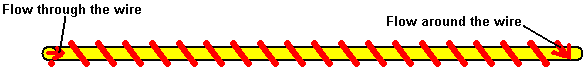 The above sketch does not show the proportions correctly, as the current flow spiralling along the outside of the wire should be hundreds of thousands of times longer than shown, which is not practical in a diagram. The actual path taken by current flow makes the surface of the wire of particular importance, and the insulation material is also of great importance. In years gone by, wire manufacturers used to anneal (cool down) copper wires in air. This created a layer of cupric oxide on the outer surface of copper wires, and that layer gave the wire different characteristics than copper wire has today. William Barbat in his patent application claims that the cupric oxide layer can be utilised in making devices with greater power output than the power input from the user. Unfortunately, the world is not quite as simple as that, as power flowing in a circuit has at least two components. The electrical current which we measure with ammeters is as described above and is sometimes referred to as “hot” electricity as when it flows through components, it tends to heat them up. But there is another component referred to as “cold” electricity, so named because it tends to cool components down when it flows through them. For example, if the output wires of Floyd Sweet’s VTA device were short circuited together, frost would form on the device due to the heavy flow of “cold” electricity, and getting a “shock” from it could give you frostbite instead of a burn. “Cold” electricity is not something new, it has always been there as it is just one aspect of “electricity”. It has not been investigated much by conventional science because none of the instruments used to measure “hot” electricity, react to “cold” electricity at all. (Actually, “hot” electricity, “cold” electricity and magnetism are all features of a single entity which should really be called “electromagnetism”). Now the spooky bit: “cold” electricity does not flow along or through the wire at all. Instead, it flows in the space around the wire, possibly riding on the magnetic field caused by the “hot” current. Thomas Henry Moray is famous for building a device which captured “cold” electricity and produced a massive power output capable of powering a whole host of ordinary electrical pieces of equipment. In his many public demonstrations before he was intimidated into silence and his equipment smashed, he invited members of the audience to bring a piece of ordinary glass with them. Then, when his circuit was powering a row of lights, he would cut one of the wires and insert the piece of glass between the cut ends of the wires. This had no noticeable effect on his circuit, with the power flowing happily through the glass and on through his circuit, powering the lights just as before. That does not happen with “hot” electricity, but as the “cold” electricity is not flowing through or along the surface of the wire, a break in the wire is not a major obstacle to it. We still do not know very much about “cold” electricity. Edwin Gray snr. demonstrated light bulbs powered by “cold” electricity being submerged in water. Not only did the bulbs continue to operate unaffected by the water, but Edwin often put his hand in the water along with the lit bulb, suffering no ill effects from doing so. Neither of those two effects are possible with conventional electricity, so please don’t try them to check it out. Another interesting item is the water-powered car system produced by Nathren Armour. His system, (among other things) involves feeding extra electrical power to the spark plugs. One thing which has always puzzled him is that the engine will not run with just one wire going to the spark plug cap. He has to have a second wire running from his extra power supply to the body of the plug where it screws into the engine block. Take that wire away and the engine stops. Put it back again and the engine runs. But according to conventional electrics, that wire cannot possibly be needed, because the engine block is grounded and the power supply output is grounded, so in theory, there is no voltage difference between the ends of the wire, therefore no current can flow along the wire, hence the wire is not needed and has no function. Well, that is true for “hot” electricity, but it is possible that the Nathren Armour system is using “cold” electricity as well as “hot” electricity and the “cold” electricity needs the extra wire as a flow guide to the spark plug. Enough about that for now. Let’s go one step further into the “weirdness” of the actual world. If, three hundred years ago, you had described X-rays, gamma rays, nuclear energy and TV signals to the average well-educated person, you would have run a considerable risk of being locked up as being mad. If you do it today, your listener would probably just be bored as he already knows all this and accepts it as a matter of fact (which it is). Please bear that in mind when you read the following information. If it seems strange and far-fetched, that is only because conventional science today is lagging badly behind and still teaching things which have been conclusively proven to be wrong decades ago. If you lived in a desert and every day a company drove in with a lorry-load of sand and sold it to you for a large amount of money, what would you think about that? Not a very good deal for you, is it? What’s that you say, you would never do that? But you already do, because you don’t realise that the sand is all around you ready for the taking at next to no cost at all. Several people have tried to publicise the fact, but the sand company has immediately silenced them by one means or another. The company does not want to lose the business of selling you the sand and definitely doesn’t want you to start picking it up for yourself for free. Well... to be perfectly fair, it is not actually sand, it is energy, and it is all around us, free for the taking. Sound a bit like X-rays did three hundred years ago? Doesn’t mean that it is not true. It is perfectly true. The design of all computers made today is based on the equations of Quantum Mechanics, and while those equations are not yet perfect, they are easily good enough for practical purposes. The snag is that the world seen at the level of the quantum is not much like the world we think that we see around us and which we think that we understand fully. Examining the world at the quantum level shows that we live in a seething mass of incredible energy. Einstein is famous for stating that Mass equals a very large amount of Energy, a fact that is shown clearly when an atomic bomb is detonated. Put in different words, a small amount of matter is the equivalent of a very large amount of energy. Actually, Energy and Matter are two different aspects of a single thing (which could reasonably be called “Mass-Energy”). At the quantum level, it can be seen that particles of matter pop into existence and drop out again into energy on a continuous basis, everywhere in the whole of the universe. The whole universe is seething with energy. That energy doesn’t bother us any more than water bothers a fish, as we evolved in this sea of energy and we just don’t notice it. It doesn’t harm us, but if we wanted, and knew how, we could use as much of that energy as we wanted for ever and ever. The amount of that energy is unbelievable. It has been calculated that one cubic centimetre anywhere in the universe contains enough energy to create all of the matter we can see in the whole of the universe. Think how many cubic centimetres there are in the Earth ... the Solar System ... our Galaxy ... If every person on Earth were to run their vehicles, power their homes, fly their planes, etc. etc. for the next million years, it would not make the slightest dent in the energy contained in one cubic millimetre of the universe. This is not a theory, it is a fact. (Would you like to buy a big pile of sand? - I’ve got a load just over here...). This big energy field has gone under different names over the years. A popular name at the present time is the “Zero-Point Energy Field” and it is responsible for everything that happens in the universe. It powers life itself. It balances out in equilibrium everywhere, which is one reason which makes it hard to realise that it is all around us. Tom Beardon is an American man with very considerable abilities and considerable in-depth knowledge of how the world actually operates. His statements are generally based on laboratory-proven criteria backed up by his high level of mathematical skills which give him an additional grasp of things. He explains how electricity actually works in circuits, and it is nothing like the system taught in schools and colleges. We think that when we attach a battery to an electrical circuit, the battery forces a current through the wires of the circuit. Sorry Chief - it is actually nothing like that at all. The power in the circuit comes directly from the Zero-Point Energy Field and has very little to do with the battery at all. We tend to think of “using up” power, but that is just not possible. Energy cannot be destroyed or “used up” the most you can do to it is to change it from one form to another. It will perform “work” (power equipment, generate heat, generate cold...) when it changes from one form to another, but if you reverse the process and convert it back to it’s original form, it will perform another lot of “work” during the conversion and end up back in exactly the same state as it started out from, in spite of having performed two lots of “work” during the operation. A battery does not provide energy to power a circuit. Instead, what happens is that the chemical action inside the battery causes negative charges to gather at the “minus” terminal of the battery and positive charges to gather together at the “plus” terminal of the battery. These two close-together “poles” of the battery are called a “dipole” (two opposite poles near each other) and they have an effect on the Zero-Point Energy Field which is everywhere. The “Plus” pole of the battery causes a massive cluster of Zero-Point Energy Field negative charges to cluster around it. In the same way, the “Minus” pole of the battery causes a massive gathering of ZPE (“Zero-Point Energy”) positive charges to gather around it. Not only do these charges gather around the poles of the battery, but an imbalance in the energy field is created and the ZPE charges continue to arrive at the poles and they radiate out in every direction in a continuous stream of incredible energy. So, there is your shiny new battery sitting there, not connected to anything and yet it causes massive energy streams to radiate out from its terminals in every direction. We don’t notice it, because the energy flows freely through us and we can’t feel it and none of our conventional instruments, such as voltmeters, ammeters, oscilloscopes, etc. react to it at all. The situation changes immediately if we connect a circuit to the battery. The circuit provides a flow path for the ZPE energy to flow along, and a significant amount of energy flows near the wires of the circuit, actually powering the circuit for a split second until it reaches the battery “pole” at the far end of the circuit. When it gets there it promptly wipes out the pole, destroying it completely. The ZPE field calms down and the energy flow ceases. But our trusty battery immediately does it all again, using it’s chemical energy to create the “dipole” once more, and the imbalance of the ZPE field starts again. It is because the battery has to use it’s chemical energy all the time, creating and re-creating, and re-creating it’s “dipole” that it runs down and eventually ceases to be able to create the dipole any more - result: no more power in the circuit. Sorry to spoil the illusion, but the battery never did power the circuit itself, it merely acted as channelling device for the Zero-Point Energy Field. In passing, Direct Current (“DC”) is actually not a continuous current at all, but instead it is a stream of DC pulses at an incredibly high frequency - way higher than we can measure at present. The speed of the pulses is so great that it looks continuous to us, a bit like the individual still pictures which are the frames of a movie, appear to be a moving image to us if they are played one after the other at a rate of 25 per second - it looks like continuous movement to us, but in reality, it is a rapid series of still pictures. The way that a battery “dipole” works on the Zero-Point Energy Field is rather like the way that a magnifying glass acts on sunlight. The rays of the sun get concentrated into a point, focused by the lens. You can start a fire with the lens, and it would be easy to think that the lens started the fire, when in actual fact, it is the rays of the sun that started the fire and the lens just influenced a local area of the large “field” of sunlight, raising the temperature at just one point. While we tend to think of a “dipole” being generated by a battery, the same effect is also created by a magnet, whether an electromagnet or a permanent magnet - remember that electricity and magnetism are two faces of the same entity. It is possible, but not easy, to capture the energy streaming out from the interference with the ZPE field caused by the poles of a magnet. For example, Hans Coler managed to do this with a completely passive device which, when set up correctly, could produce electrical power, hour after hour from apparently “nothing” (well, actually, the ZPE field). Roy Meyers also did it with his patented array of magnets and zinc plates - completely passive, with no moving parts at all, no battery and no circuitry. Patrick Kelly engpjk@yahoo.co.uk http://www.free-energy-info.co.uk/ |